
Compound Semiconductor Wafer & Epitaxy Supplier | Power Wafertech Group

PRODUCT CENTER

Find the right wafer for your program.

Explore our standard compound semiconductor substrates and epi wafers—or collaborate with our engineers for custom specifications.

Get Technical Support

Product Search & Classification

Search by Material. Refine by Specification.

Quickly locate standard compound semiconductor wafers, or request a custom spec for your device program.

III-V Semiconductor Epitaxial Wafers

III-V Semiconductor Epitaxial Wafer

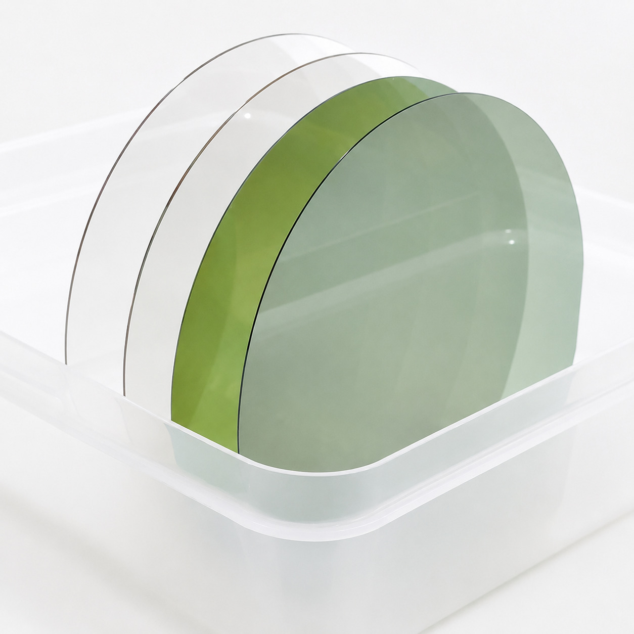
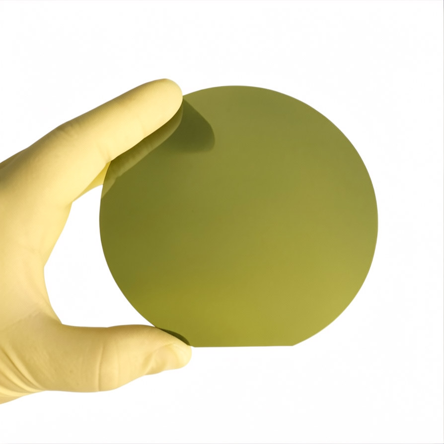
Precision MOCVD/MBE-grown heterostructures on InP, GaSb, and GaAs substrates. Engineered for high-performance HEMTs, pHEMTs, HBTs, laser diodes, VCSELs, and IR detectors. Supporting custom epi structures from R&D to volume production.
View Product

SiC Wafers

SiC Substrate

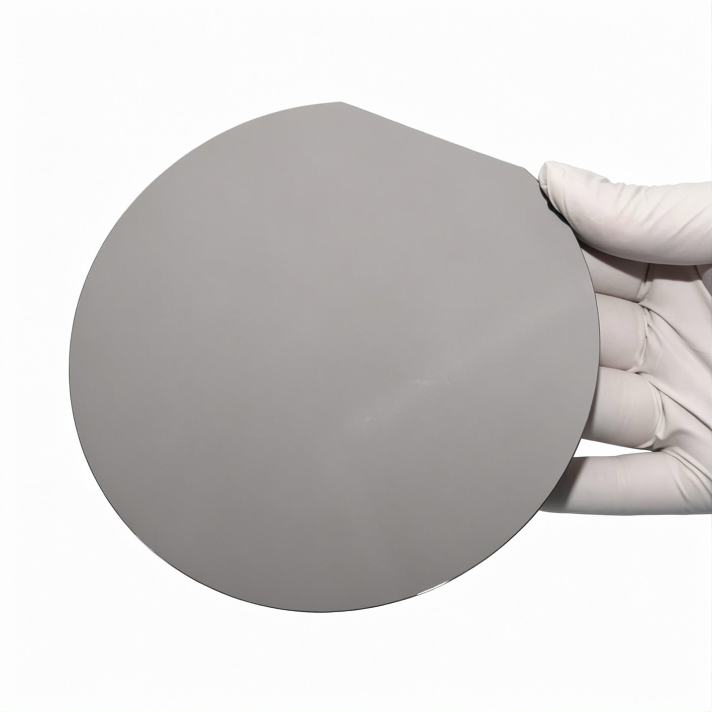
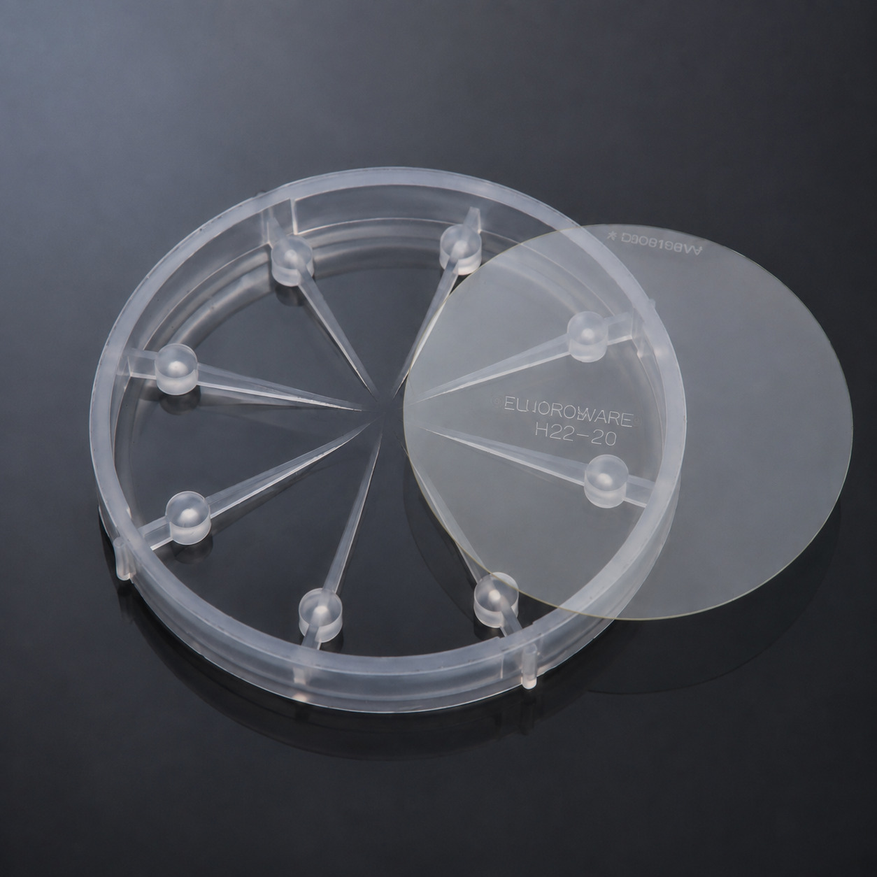
SiC substrate wafers for power, RF, optoelectronic and advanced semiconductor applications. Available in 4H-SiC, 6H-SiC and 3C-SiC, with N-type, P-type and semi-insulating options, multiple wafer sizes, doping levels and surface finishes.
View Product

SiC Wafers

SiC Epitaxy

Our SiC epitaxial wafers – grown by CVD on SiC substrates – provide well-controlled uniformity and low defect density, forming a reliable platform for SBD, MOSFET, JFET, IGBT, GTO, BJT and so on from 600V to 10kV.
View Product

AlN Template

AlN on Silicon Template

AlN on silicon templates provide a high-quality interface and buffer platform for subsequent GaN epitaxy, supporting the development of high-performance GaN power and RF devices.
View Product

AlN Template

AlN on Sapphire Template

Sapphire based AlN templates are available in multiple wafer sizes and customizable AlN thicknesses and orientations, AlN-on-sapphire templates with high crystalline quality and low defect density are suitable for both R&D and device production development.
View Product

THREE CORE MATERIAL FAMILIES

Engineered Materials for Your Device Roadmap

Browse substrates and epi wafers by material family. Standard configurations and custom specifications available for R&D and volume production.

APPLICATIONS & INDUSTRIES

Applications & Industries

CASE 01 / HIGH-VOLTAGE SYSTEMS

Power Electronics

Wide-bandgap wafer solutions engineered for 800V+ architectures. Ensuring high-efficiency power conversion, fast switching, and reliable high-temperature operation.

APPLICATION FOCUS

EV powertrains · fast charging · industrial motor drives

RECOMMENDED PRODUCTS

4H-SiC GaN

ENGAGEMENT PROCESS

How a custom inquiry moves forward

Submit your program-specific requirements and our engineers will take them from evaluation to a confirmed quote.

CUSTOM ENGINEERING

Parameters beyond the standard list

Custom diameter & thickness
Orientation & off-cut
Doping & resistivity
Thin films & layer stacks
Surface & edge profile
Marking & packaging
01Submit requirements
02Engineering review
03Specification alignment
04Quote & lead time
Talk to an Engineer

TECHNICAL INQUIRY

Speak to Engineers About Your Wafer Needs

Share your material, dimensions, specifications, application or project stage. Our team will review your requirements and respond within one business day.

Engineering-led response

Inquiries are routed to the appropriate technical or commercial team.

Address

No. 1389, Lianmei Road, Lianhua Industrial Zone, Tong’an, Xiamen, Fujian 361100, China

File Upload
Emailvictorchan@powerwafertech.com Phone+86-592-5633652