
01
Crystal Growth
Precise doping control and low defect density (PVT, LEC, VGF)

About Power Wafertech Group
Discover PWG's full-cycle manufacturing capabilities for compound semiconductor substrates and epi wafers. Delivering engineering collaboration from R&D to high-volume production.
Company Overview
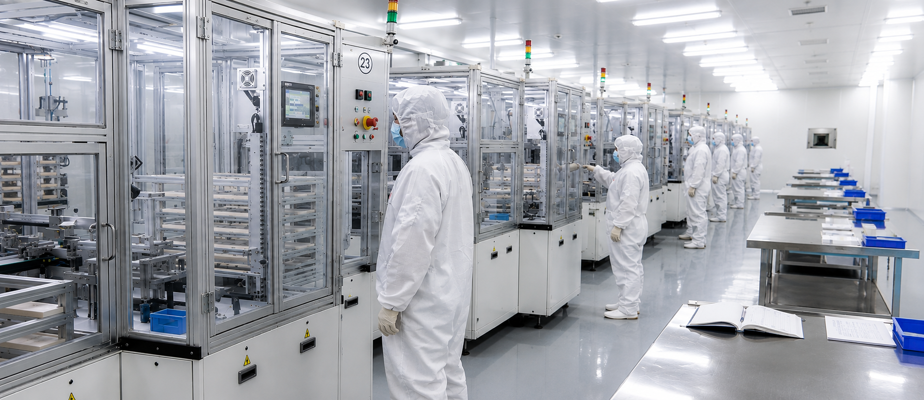
Power Wafertech Group is a full-cycle material manufacturer of compound semiconductor substrates and epitaxial wafers, including SiC, GaN, InP, GaAs, GaSb, and InSb. We control the core processes—from crystal growth and substrate fabrication to epitaxial deposition—ensuring supply chain security and strict material consistency.
We support global customers with strict specification adherence, complete batch traceability, and rapid engineer-to-engineer support. From R&D prototyping to repeat production, we deliver documented, high-quality materials for your device programs.
Technology & Manufacturing
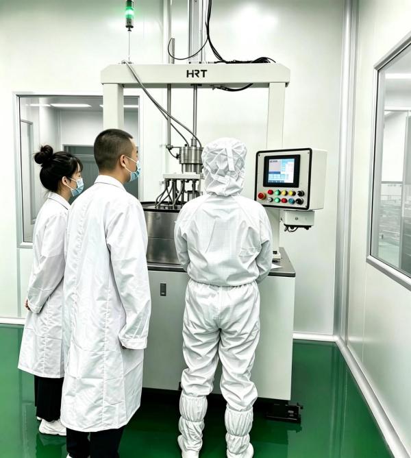
A fully controlled, in-house manufacturing flow. We ensure strict quality control, full batch traceability, and secure supply at every stage of your device program.
01
Precise doping control and low defect density (PVT, LEC, VGF)
02
Advanced slicing, grinding, and CMP polishing for Epi-ready surfaces
03
HVPE / MOCVD / MBE growth with tight thickness and doping uniformity
04
Downstream processing including wafer dicing, thinning, and metallization
05
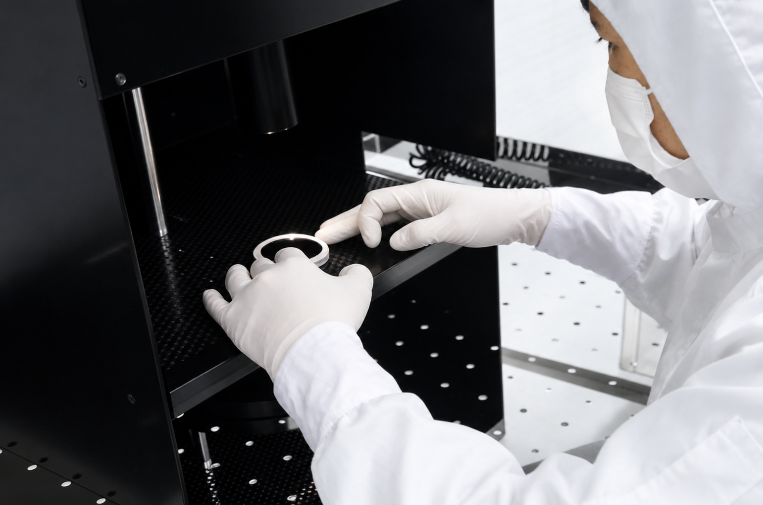
Comprehensive inspection using XRD, AFM, and PL mapping. Complete CoA provided.
WAFER SERVICES
A complete portfolio of precision processing and thin-film deposition services. We deliver tailored solutions from substrate processing to complex device fabrication, ensuring performance meets your exact project needs.
High-accuracy CMP polishing, dicing, and wafer thinning for 4H-SiC, GaSb, InSb, and other wide bandgap/III-V materials.
Optical and electrical coatings via e-beam evaporation or sputtering. High-adhesion metals (Au, Ti/Pt/Au) and IR/UV anti-reflection films.
Advanced bonding solutions including 4H-SiC-on-Insulator (4H-SiCOI) for high-performance RF, power devices, and integrated photonics.
Precise control over species, energy, and dose to form conductive or isolation regions in SiC, GaN, Si and other compound semiconductors.
Quality & Inspection
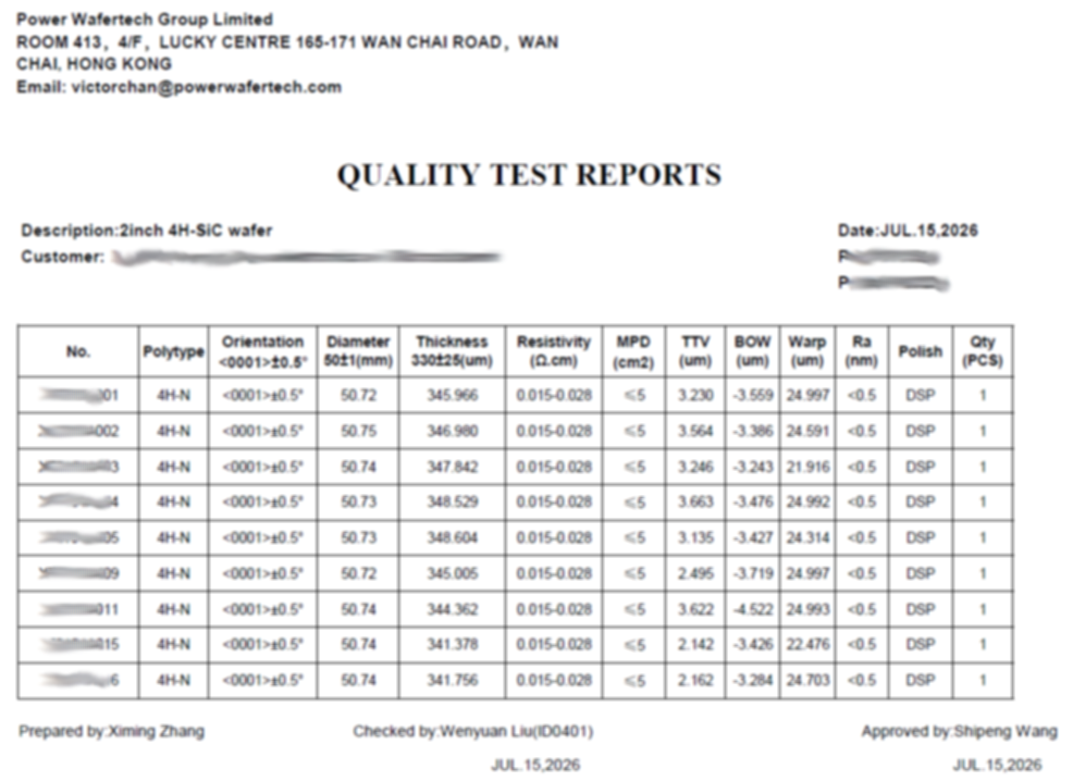
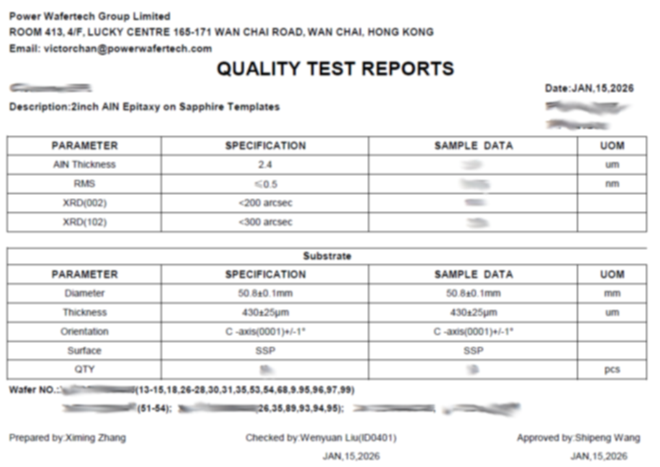
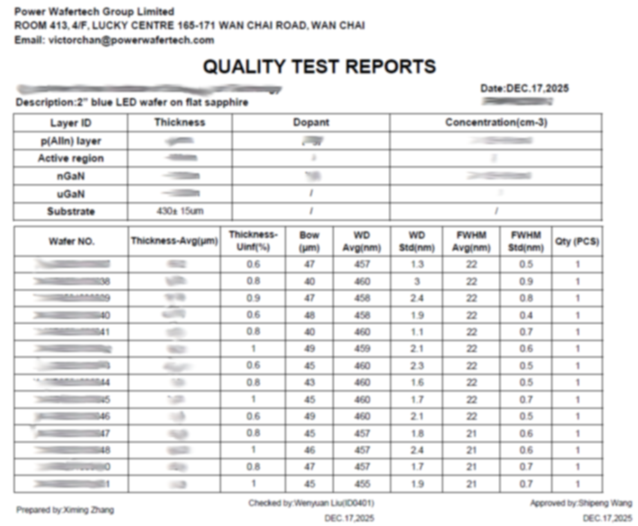
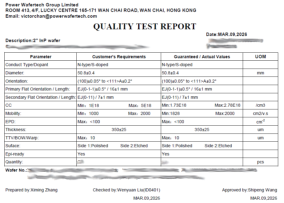
Quality expectations are aligned at specification review and supported through incoming, in-process and outgoing controls. Available reports, traceability fields and packaging options are confirmed per product and order.
Quality Test Reports
Collaboration Evidence
Representative examples of how we support industry and research programs. Detailed project data and client identities are protected under strict NDAs.
Industry Program
Scaling validated substrate specs to high-volume production.
Precision CMP polishing, wafer thinning, and high-volume dicing for 4H-SiC. Delivering Fab-ready substrates with strict batch consistency.
Research Program
Low-volume custom epitaxy for novel device characterization.
Rapid prototyping and custom epitaxy with low MOQ. MOCVD/MBE growth of multi-layer stacks coupled with full material characterization.
Application Development
Customized doping and surface treatment for emerging architectures.
Precision ion implantation and tailored metal coatings for device isolation and ohmic contacts.
Facilities & Global Support
View each site's business scope. Facility information is documented subject to formal validation.
Base 01
In-house crystal growth and material synthesis
Base 02
Slicing, grinding and polishing
Base 03
Advanced epitaxy growth and thin-film deposition
Base 04
Special formats, QA and program support
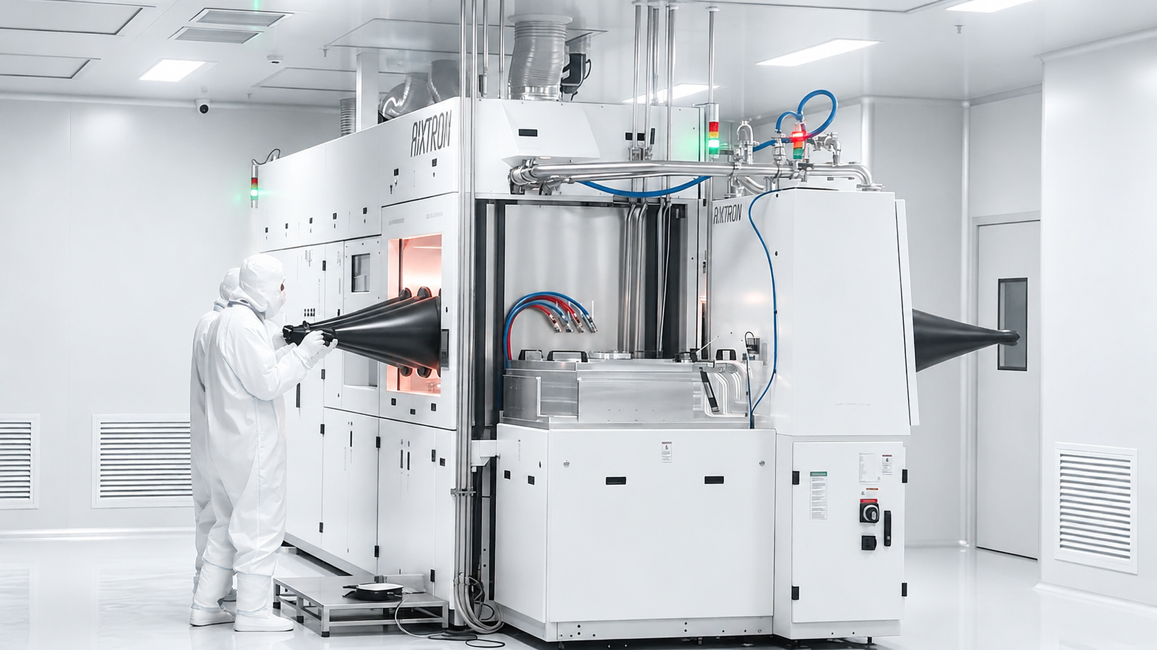
ISO-certified cleanrooms equipped for crystal growth, wafer fabrication, and epitaxial deposition.
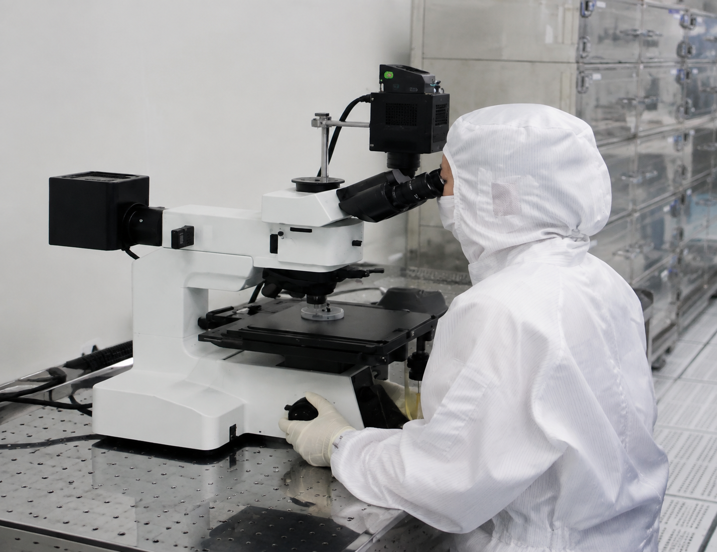
Equipped with XRD, AFM, and PL mapping for rigorous material characterization and inspection.
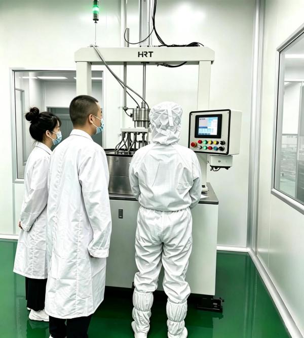
Securing global supply chains with strict batch traceability, NDA-protected engineering support, and secure cleanroom packaging.
Work with Power Wafertech
Explore our wafer portfolio or discuss a material, processing or program requirement with our team.


