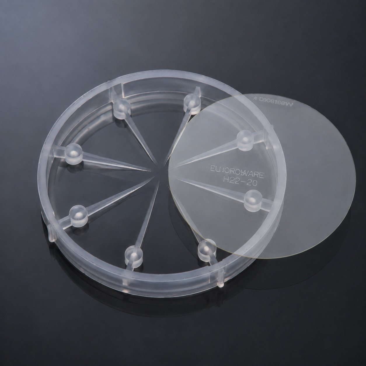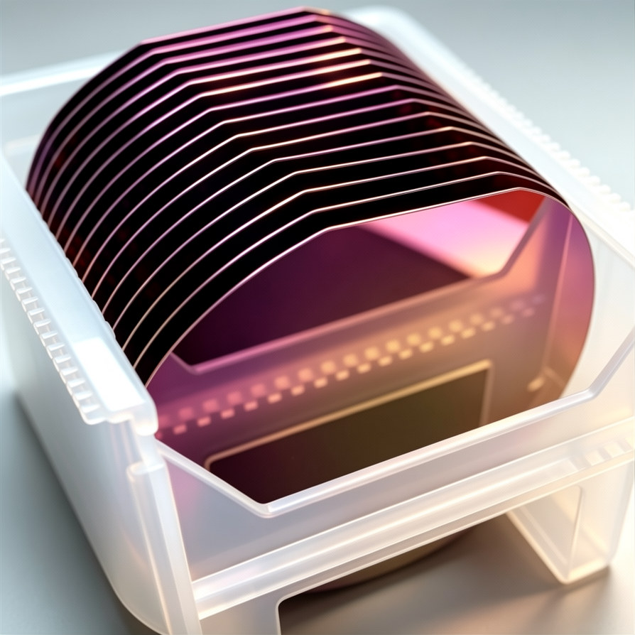

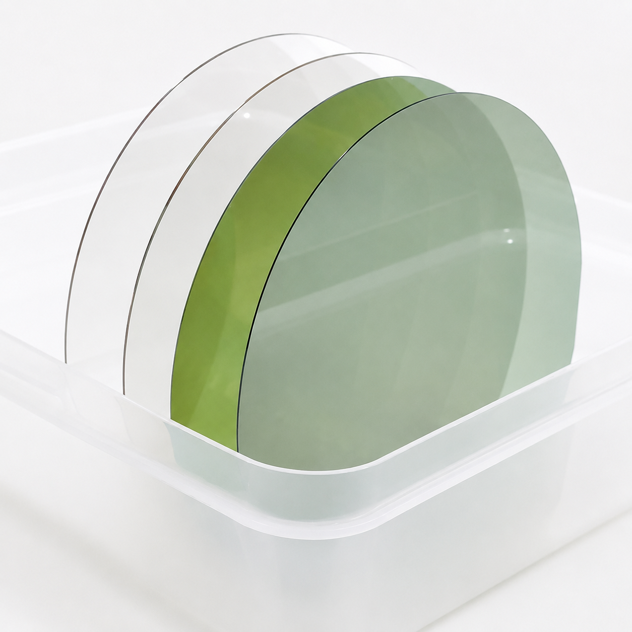
The 8-Inch SiC Inflection Point: What 2026 Means for Substrate and Epitaxy Buyers
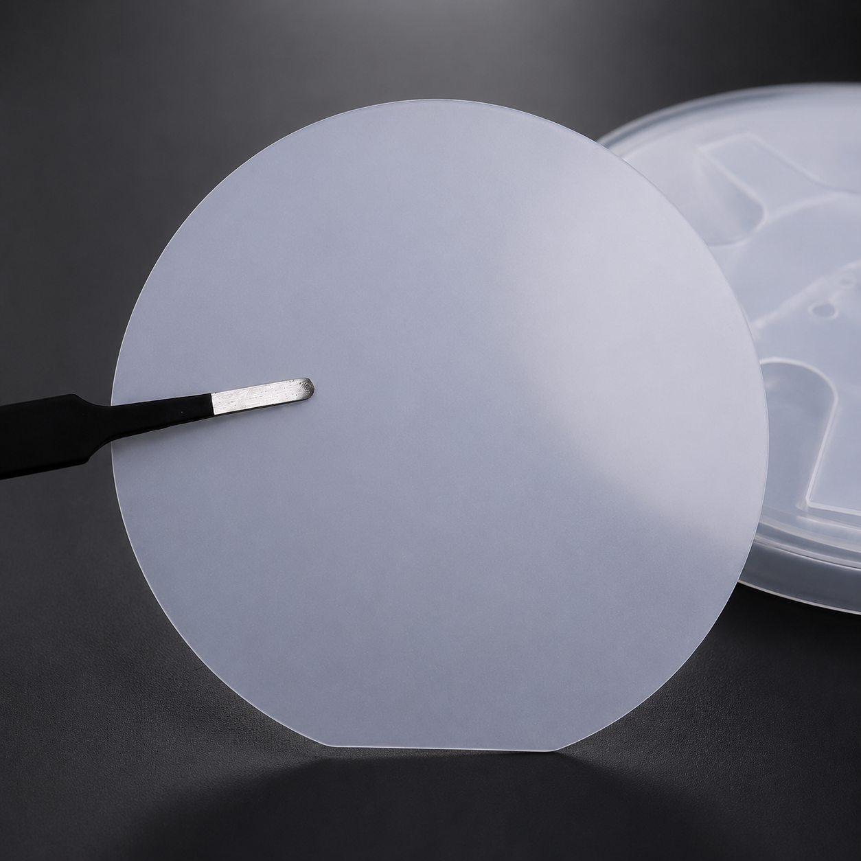
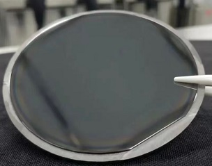
8-inch SiC substrates are moving from pilot to mainstream. Explore 2026 supply, pricing and epitaxy implications for power device makers.
2026-09-01 14:19:48
Read Article
8-inch SiC substrates are moving from pilot to mainstream. Explore 2026 supply, pricing and epitaxy implications for power device makers.
AI racks are moving from 10 kW to over 100 kW. See how 800 V HVDC architecture splits demand between SiC and GaN, and what it means for epiwafer specs.
Spacer-layer thickness strongly affects cryogenic noise in InP HEMTs, with an optimized value balancing mobility, gate control, and real-space transfer. Cap-layer doping and stability must also be co-designed with metallization and lift-off processes to keep contact resistance low.
Explore TFLN (thin-film lithium niobate) wafers for integrated photonics, electro-optic modulation, and SAW applications, with customizable crystal orientations, and film thicknesses.
β-Ga₂O₃ Substrates for DUV Detection & Radiation Devices
Global silicon wafer shipments reached 3,573 MSI in Q2 2026, up 7.4% year on year. What the latest SEMI data means for supply, lead times and qualification.
Share a specification, request evaluation samples or speak with our engineering team about your application.
Request a Quote