

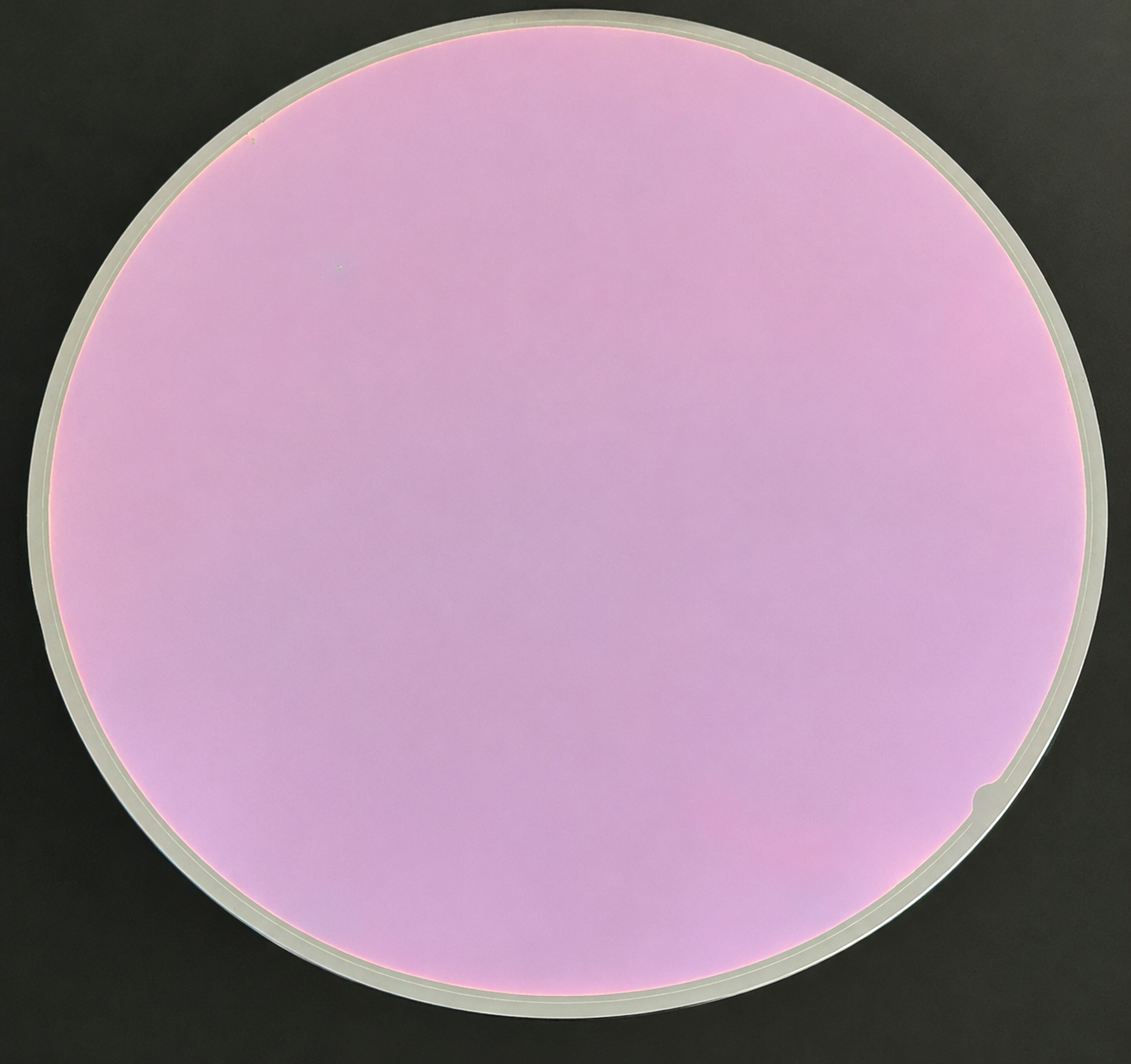
Thin-film lithium niobate (TFLN) has become an important materials platform for integrated photonics, high-speed electro-optic modulation, nonlinear optics and advanced surface acoustic wave (SAW) devices. By combining the strong electro-optic and piezoelectric properties of single-crystal lithium niobate (LiNbO₃) with a thin-film structure, TFLN technology enables compact device architectures and greater integration flexibility.
For researchers and device manufacturers, wafer selection involves more than the lithium niobate film itself. Crystal orientation, film thickness, buried oxide (BOX) thickness, supporting substrate, surface quality and thermal behavior can all influence fabrication yield and device performance.
1. What Is TFLN? Understanding the LNOI Wafer Structure
TFLN stands for thin-film lithium niobate. It generally refers to a thin, single-crystal LiNbO₃ layer used to fabricate integrated photonic and electro-optic devices.
A common implementation is lithium niobate on insulator (LNOI), which typically consists of three layers:
- Top layer: A single-crystal LiNbO₃ thin film that provides electro-optic, nonlinear optical and piezoelectric functionality.
- Buried oxide layer: Usually silicon dioxide (SiO₂), providing electrical and optical isolation.
- Handle substrate: Commonly silicon (Si), with other supporting materials available for specific platform designs.
This layered structure supports compact optical waveguides, high-density photonic integration and device fabrication using thin-film processing techniques.
Although TFLN and LNOI are closely related terms, they are not strictly interchangeable in every context. TFLN describes the thin-film material platform, whereas LNOI commonly identifies the lithium-niobate-on-insulator wafer architecture.
It is also important to distinguish standard TFLN wafers from chemically reduced or blackened LiNbO₃. Blackening is a separate material treatment intended to modify electrical conductivity and optical absorption; it is not an inherent feature of every TFLN wafer.
2. TFLN Wafer Specifications and Customization Options
Power Wafertech Group provides silicon-based lithium niobate thin-film wafer solutions for research and device development. X-cut, Y-cut and Z-cut configurations, along with structural and thickness requirements, can be discussed according to the intended application.
| Parameter | Representative options |
|---|---|
| Material | Single-crystal lithium niobate (LiNbO₃) |
| Wafer structure | LiNbO₃ thin film / SiO₂ / silicon |
| Wafer diameter | 3 in, 4 in, 6 in; 8 in for selected platforms |
| Crystal orientation | X-cut, Y-cut, Z-cut |
| LiNbO₃ film thickness | Approximately 300–900 nm for common photonic platforms |
| Buried oxide thickness | Commonly around 1–4 µm, depending on design |
| Handle substrate | Silicon |
| LN composition | Congruent LN; stoichiometric LN or MgO-doped LN subject to availability |
| Surface condition | Device-grade polished surface; roughness and inspection criteria to be specified |
| Wafer geometry | Total thickness, TTV, bow, warp and local thickness uniformity |
| Bonding interface | Bonding integrity and void inspection requirements to be confirmed |
| Customization | Film thickness, orientation, BOX thickness and substrate configuration |
Note: The figures above are general reference ranges. Actual availability, tolerances and quality criteria should be confirmed for the required wafer diameter and structure.
Key Considerations for Wafer Selection
- Crystal orientation: X-cut, Y-cut and Z-cut lithium niobate wafers provide different relationships between the crystal axes, optical modes and applied electric fields. The appropriate cut depends on the device architecture.
- Film thickness: Thin-film thickness influences optical confinement, waveguide geometry and device performance. The target thickness should be selected according to the operating wavelength and fabrication design.
- Buried oxide thickness: The SiO₂ layer affects optical leakage into the supporting silicon substrate and should be specified for the intended device.
- Surface and interface quality: Surface roughness, thickness uniformity, bonding integrity and wafer geometry can affect lithography, etching and device consistency.
Power Wafertech Group welcomes inquiries regarding lithium niobate thin-film wafers for research, prototyping and device development.
3. Pyroelectric Effects in Lithium Niobate
Lithium niobate is a ferroelectric and pyroelectric material. Temperature changes can alter its spontaneous polarization, generating surface charge. If the charge cannot dissipate rapidly, electrostatic fields may accumulate and interfere with wafer processing or device operation.
Congruent lithium niobate (CLN) typically has a Li/Nb ratio of approximately 48.5:51.5. Its low room-temperature DC conductivity, reported at around 10⁻¹⁸ Ω⁻¹ cm⁻¹ under specific conditions, can contribute to persistent surface charging.
These effects are relevant to temperature-dependent SAW devices, lithography, electrode fabrication and repeated thermal cycling. The actual behavior depends on crystal composition, surface condition, temperature history and electrical boundary conditions.
4. Chemical Reduction of Lithium Niobate for Charge Control
Chemical reduction, commonly called blackening, modifies the defect state of lithium niobate and can increase its electrical conductivity and optical absorption. This treatment has been investigated as a method for reducing pyroelectric charge accumulation and suppressing backside reflection during photolithography.
In reported experiments, chemical reduction increased CLN conductivity by more than five orders of magnitude. Following a 120°C-to-80°C temperature cycle, a wafer reduced at 394°C exhibited a surface electric field below the measurement limit, while untreated CLN produced a field approaching 2 kV/cm under the same test conditions.
A separate 78 MHz SAW filter study reported no corresponding pyroelectric discharge pulses from the blackened device under the test conditions. However, its insertion loss was approximately 0.5 dB higher at 70°C than that of the untreated reference.
These findings indicate that blackening can improve charge dissipation, but the treatment level must be optimized to balance electrical performance and device loss.
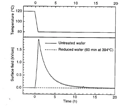
Fig. 1 — Comparison of wafer temperature and surface electric field during thermal cycling for blackened and untreated congruent lithium niobate (CLN)
Optical Absorption and Lithography
Chemical reduction also increases optical absorption in lithium niobate. In reported experiments, a broad absorption feature appeared around 500 nm. Wafers reduced at 592°C or above exhibited more than 95% attenuation of near-ultraviolet light over a 0.7 mm double-pass optical path.
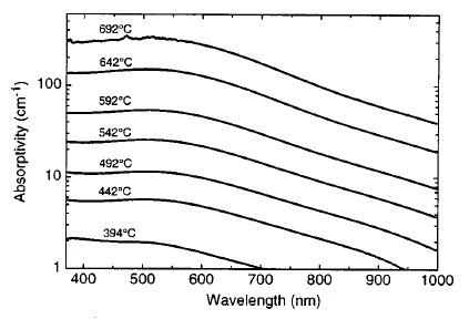
Fig. 2 — Optical absorption spectra of lithium niobate after chemical reduction at different temperatures, illustrating the temperature-dependent change in optical absorption
This property can help suppress wafer backside reflection during photolithography and lift-off, potentially improving exposure contrast and electrode linewidth uniformity.
However, blackening can significantly reduce transmission in the 1–5 µm wavelength range. Untreated optical-grade lithium niobate may therefore be more appropriate for applications requiring high near-infrared or mid-infrared transmission.
The reduction conditions described in research publications are experimental references rather than universal processing recommendations. Treatment suitability must be validated for the specific wafer and application.
5. CLN vs. NSLN: Choosing the Right Lithium Niobate Material
Congruent lithium niobate (CLN) and near-stoichiometric lithium niobate (NSLN) offer different approaches to material optimization.
CLN is widely used in electro-optic, acoustic and nonlinear optical research. Chemical reduction can modify its conductivity and absorption, making it relevant to pyroelectric charge control and lithography-related applications.
NSLN has a lithium-to-niobium ratio closer to 1:1 and generally exhibits a lower concentration of certain intrinsic defects. Depending on the material and device design, it may offer advantages in electro-optic response and domain engineering.
Material selection should be based on device-level requirements rather than assuming that one composition or treatment is universally superior.
References
- Bordui, P. F., Jundt, D. H., Standifer, E. M., & et al. (1999). Chemically reduced lithium niobate single crystals: Processing, properties and improved surface acoustic wave device fabrication and performance. Journal of Applied Physics, 85(7).
- Protektor, D. O., & Lisin, D. O. (2022). Simulation of Heat Transfer in Single-Crystal Lithium Niobate in Interaction with Continuous-Wave Laser Radiation. East European Journal of Physics, 1, 10–15.
- Zhang, Y., Xiao, X., Chen, J., & et al. (2025). Lithium Niobate Crystal Preparation, Properties, and Its Application in Electro-Optical Devices. Inorganics, 13(9).