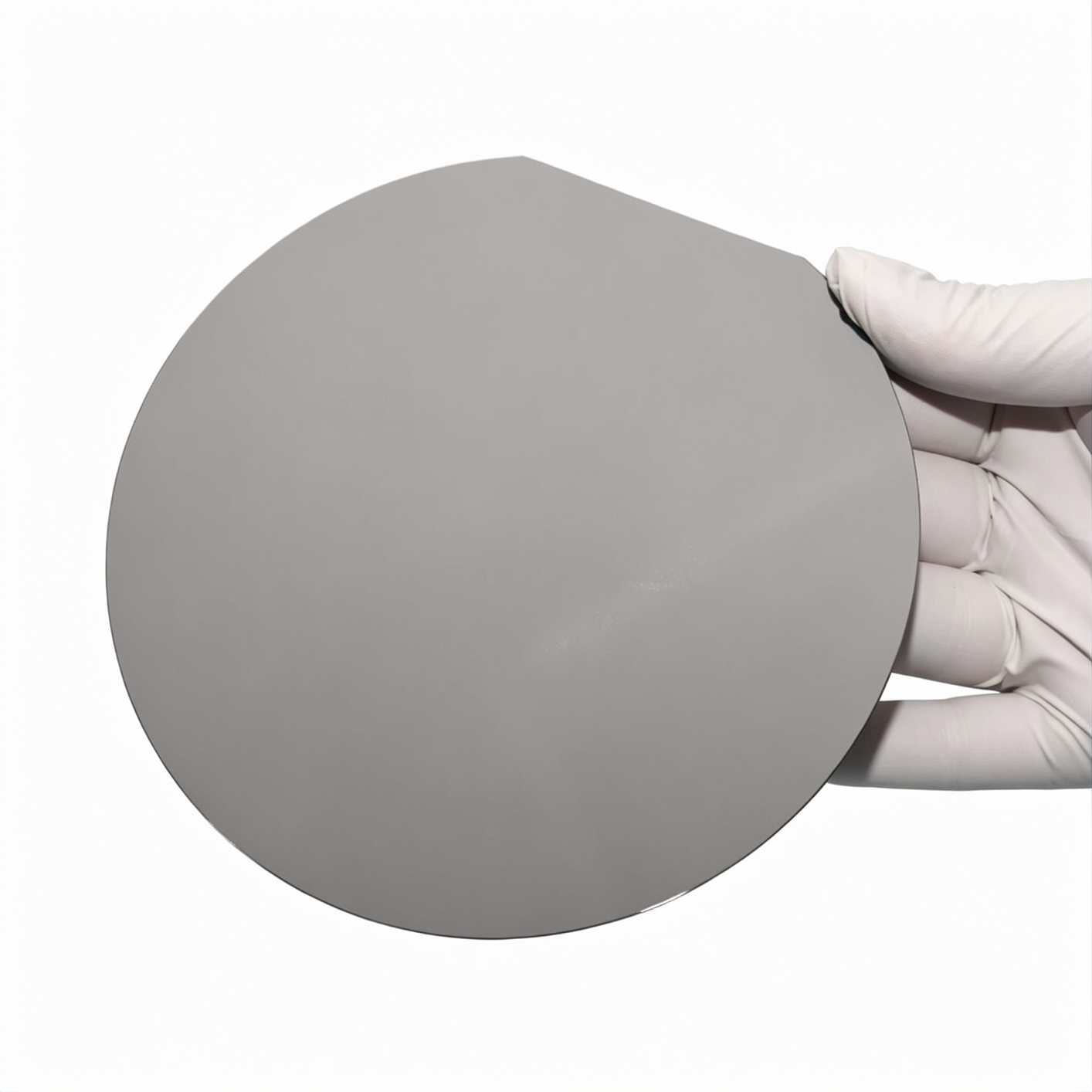
Silicon Wafer RCA Standard Cleaning
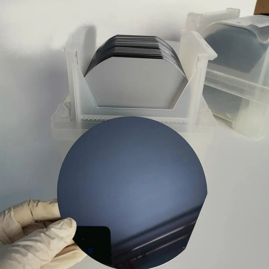
Learn silicon wafer RCA cleaning steps and key parameters. PWG supplies 2–12" prime/research/dummy grade Si wafers with technical support
2026-09-01 11:40:20
Read ArticleLearn silicon wafer RCA cleaning steps and key parameters. PWG supplies 2–12" prime/research/dummy grade Si wafers with technical support
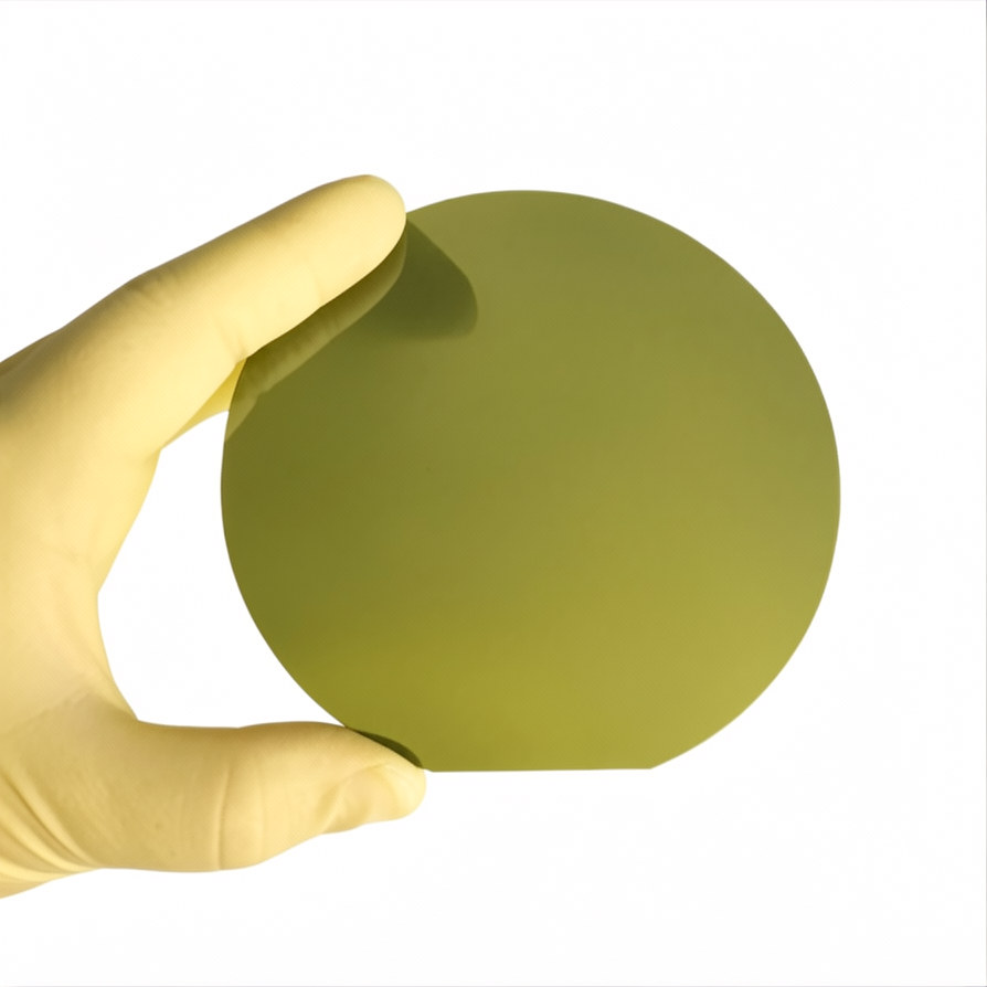
Offer various commercial epitaxy GaN photodetector wafers with customizable structures, covering different substrates and application requirements
Custom InAlN/GaN HEMT epiwafers on sapphire, SiC, and Si substrate, with high-density 2DEG, ideal for Millimeter-Wave Applications
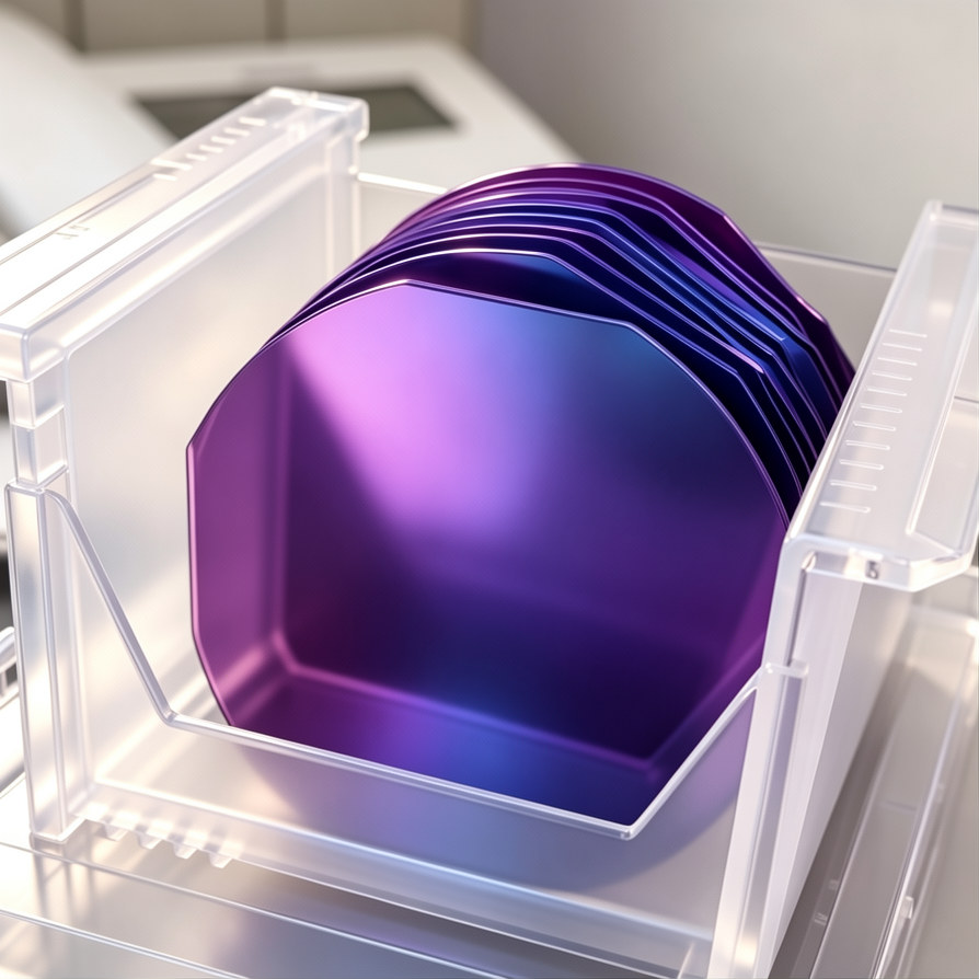
High-performance GaN based violet laser diode epiwafers supplied are grown Si substrate by MOCVD method with multi quantum wells for low threshold current.
As a professional silicon wafer supplier, PWG masters the control of Crystal Originated Particle (COP) defects, ensuring crystal integrity & yield for your ULSI devices
Discover PWG's 4H-SiC PIN diode epiwafers with optimized epilayer design, ensuring high reliability for power electronics
Share a specification, request evaluation samples or speak with our engineering team about your application.
Request a Quote