

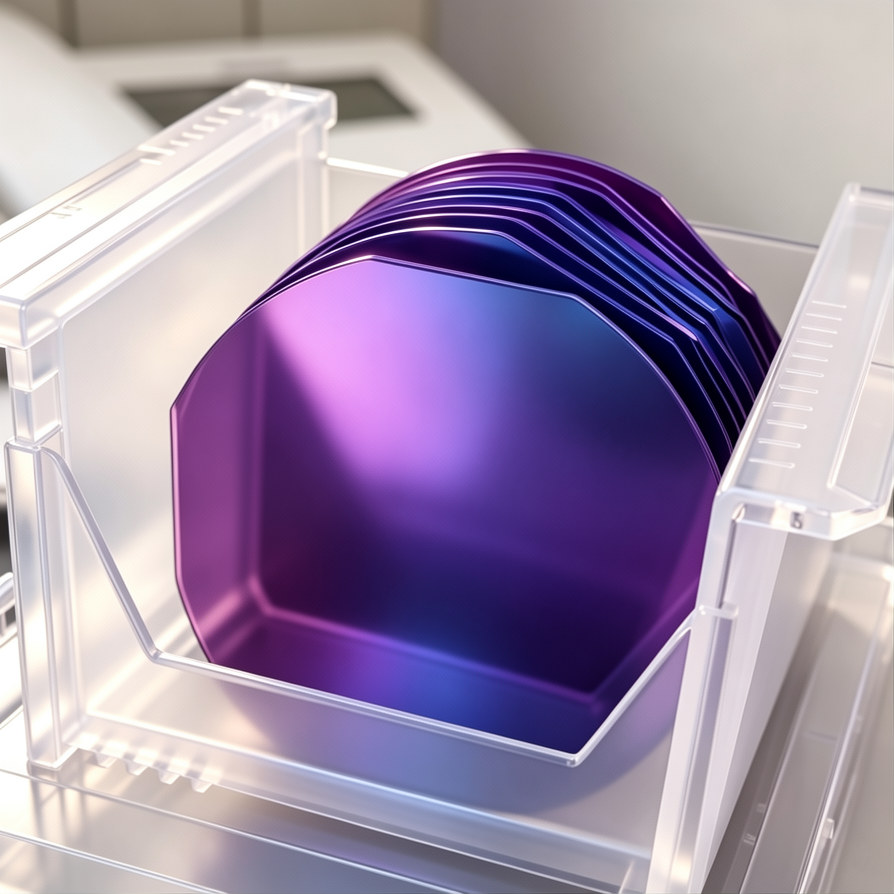
In the relentless pursuit of Moore’s Law, the semiconductor industry places ever-increasing demands on the quality of the starting material—the silicon wafer. For manufacturers of Ultra-Large-Scale Integration (ULSI) devices, minimizing defects is paramount to achieving high yields and device reliability. Among the various crystalline imperfections, Crystal Originated Particles (COP defects) stand out as a critical challenge that distinguishes a standard wafer from a high-performance one.
1. What Are COP Defects and Why Do They Matter?
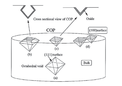
COP defects are nanometer-scale void defects—specifically, octahedral-shaped vacancies—that form within a silicon crystal during the Czochralski (CZ) growth process. They are not surface contaminants; rather, they are an inherent crystallographic feature embedded in the bulk of the material.
These voids are typically 100-200nm in size and become visible on the wafer surface as etch pits after specific cleaning processes like the Standard Clean 1 (SC-1) solution.
A crucial insight from the industry is that these defects were historically misidentified. Due to their morphology, they were first detected as LPDs (Light Point Defects) by particle counters and were long mistaken for surface contaminants introduced during wafer processing. It was not until 1990 that research revealed their true origin: they are crystallographic defects formed during crystal growth, leading to their classification as COPs.
2. Why Standard Cleaning Fails to Eliminate COPs?
A critical characteristic of COP defects is that they are not removable by standard wafer cleaning processes. In fact, as shown in numerous studies, repeated SC-1 cleaning cycles can actually increase the observed COP density. This occurs because: Existing surface COPs are not dissolved; The etchant penetrates and widens subsurface micro-voids, causing new COPs to emerge on the surface.
This phenomenon underscores the fact that COP control must be achieved during the crystal growth stage, not through subsequent wafer processing. It is a fundamental material quality issue.
3. How We Engineer Low-COP Silicon Crystals from the Start?
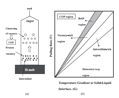
For over 30 years, the semiconductor material science community has leveraged the foundational research of Voronkov, Falster, and others to understand and ultimately control the formation of these defects. The key lies in the ratio of the crystal pulling rate (V) to the axial temperature gradient at the solid-liquid interface (G).
According to the Voronkov model, the type and density of point defects incorporated into the growing crystal are determined by the V/G ratio:
High V/G (Vacancy-Rich): Promotes vacancy agglomeration, leading to the formation of COP voids.
Low V/G (Interstitial-Rich): Leads to the formation of interstitial-type defects.
4. Proven: Magnetic Field Technology Cuts COP Density Dramatically
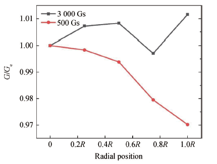
Recent advancements, as detailed in studies on 12-inch (300mm) CZ growth, highlight the critical role of transverse magnetic fields. By applying a powerful magnetic field (e.g., 3000Gs), the turbulent melt convection can be effectively dampened. This results in:
A More Stable Melt Flow: Suppresses temperature fluctuations and ensures a stable flow regime near the crystal growth interface.
Improved Temperature Homogeneity: Creates a more uniform temperature distribution within the silicon melt.
A More Uniform Temperature Gradient (G): As demonstrated in the process simulations, a higher magnetic field strength leads to a significantly more stable and uniform radial temperature gradient (G/Gc) across the solid-liquid interface.
4. COP Elimination Paths
The mainstream technological paths for eliminating COPs in recent years include:
(1) Generate nitrogen doped silicon single crystals;
(2) Hydrogen or argon annealing eliminates surface COP defects;
(3) Adjust the longitudinal temperature gradient of the thermal field to reduce the density and size of COP defects.
5. Our Solution: Delivering Low-Defect Silicon Wafers
As a professional silicon wafer supplier, PWG supply COP-free silicon wafers, wafer details as below:
| Parameters | Specification |
|---|---|
| Diameter | 300mm (12 inch) |
| Orientation | (100), (110), (111) |
| Growth Method | CZ |
| Conductivity | P type, N type |
| Resistivity | Typical 1 – 100Ω·cm |
| Surface Finish | DSP, SSP |
| Chamfer | Complies with SEMI standards |
| Packaged | Multi wafer box |
Contact our sales team now to discuss your requirements and request a quote. Let’s work together to build the future of electronics.
References
1. SHIMIZU, H., & INOUE, T. (2017). Summary of Crystalline Defects Control in Silicon. J. Coll. Eng. Nihon Univ, 59(1).
2. WANG, Z., ZHANG, Y., LIU, T., NI, H., RUI, Y., MA, C., WANG, L., CAO, Q., & YANG, S. (2025). Effect of Magnetic Field Strength on the Uniformity of COP Defects in 12 Inch Cz Monocrystalline Silicon. Journal of Synthetic Crystals, 54(12), 2101–2111.
Discuss a substrate requirement with our team
Power Wafertech supplies COP-free silicon and other advanced semiconductor wafers tailored to your device specifications. Reach out to explore crystal growth and substrate solutions for your next project.
Contact Our Team