

Silicon-based power devices are approaching their theoretical limits, and silicon carbide (SiC) has emerged as the core material for next-generation power electronics owing to its high breakdown electric field, high saturation velocity, and high thermal conductivity. Unipolar devices (e.g., Schottky barrier diodes and MOSFETs) have their specific on-resistance constrained by the unipolar limit, where the drift-layer resistance increases with the square of the breakdown voltage. In contrast, bipolar devices such as PIN diodes leverage conductivity modulation to significantly reduce high-voltage conduction losses. A PIN diode consists of a p-type anode, a low-doped n-type drift layer, and an n-type substrate, and the epilayer quality directly affects its on-state performance, switching characteristics, and reliability.
1. SiC PIN Epitaxial Structure and Design
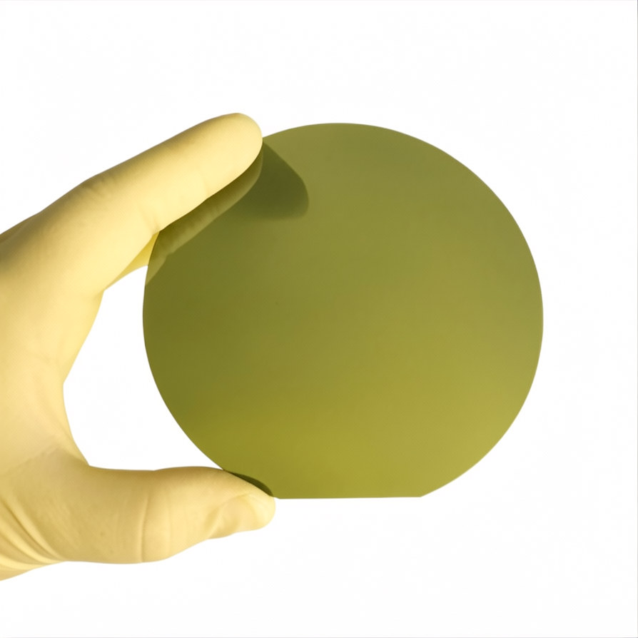
PWG can provide high-quality 4H-SiC PIN diode epiwafers, typically fabricated by homoepitaxial growth on n-type substrates with sequential deposition of a buffer layer, a drift layer, and a p-type contact layer. The doping concentration and thickness of each layer must be optimized according to the target voltage rating and on-state performance. Taking a typical product structure as an example, the epiwafer comprises:
| Epilayer | Material | Thickness | Doping |
|---|---|---|---|
| Contact Layer | P+ | 1μm | * |
| Drift Layer | N- | * | * |
| Buffer Layer | N+ | * | * |
| Substrate | N Type SiC |
2. Defect Distribution in SiC Epilayers and Its Impact on Conductivity Modulation
2.1 Comparison of Defect Characteristics between Ion Implantation and Epitaxial Growth
Deep-level transient spectroscopy (DLTS) and cathodoluminescence (CL) are effective techniques for characterizing defect distribution in epilayers. Fukaya et al. (2021) compared PIN diodes fabricated using two types of p-layer formation: one with an epitaxially grown p-layer (epi-PIN) and the other with aluminum ion implantation (impla-PIN). The results showed that impla-PIN devices exhibited significantly higher deep-level concentrations in the drift layer (at about 6μm from the junction depth) than epi-PIN devices, and the concentrations of these levels (e.g., PI1 and PI2, corresponding to Al-related defects) decayed exponentially with distance from the junction. In contrast, the deep-level concentrations in epi-PIN devices (e.g., the Z₁/₂ center) were uniformly distributed throughout the drift layer, remaining on the order of 10¹¹–10¹³cm⁻³.
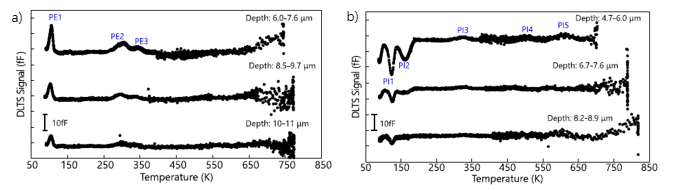
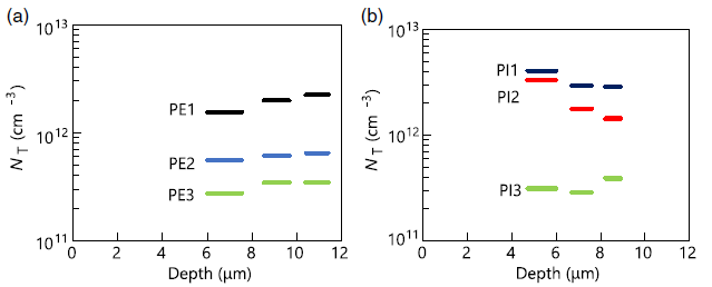
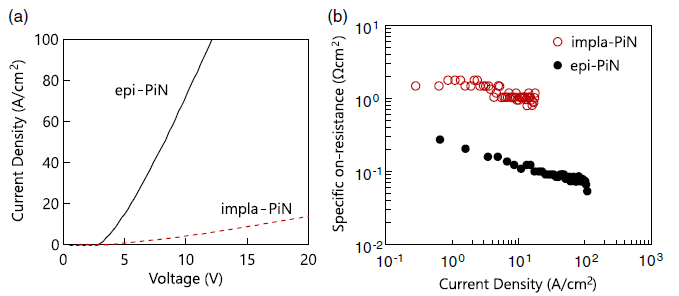
More importantly, the epi-PIN devices exhibited pronounced conductivity modulation, with a differential specific on-resistance of approximately 0.1Ω·cm², which is lower than the unipolar theoretical value of 0.24Ω·cm². In contrast, the impla-PIN devices showed a specific on-resistance as high as 1.0Ω·cm², far exceeding the theoretical value, indicating that defects introduced by ion implantation significantly suppressed minority carrier lifetime and conductivity modulation efficiency. Cathodoluminescence spectra further confirmed that the defect-related luminescence intensity in impla-PIN decreased rapidly from the junction toward the deeper region, consistent with the decay trend of defect concentration measured by DLTS.
2.2 Implications of Defect Distribution for 4H-SiC PIN Epilayer Design
The above studies indicate that aluminum ion implantation not only causes damage near the implanted region but also generates point defects and complex defects that can diffuse several micrometers or even deeper (about 10μm) into the drift layer. Even at 6μm from the implanted region, defect concentrations remain on the order of 10¹²cm⁻³, which is sufficient to reduce carrier lifetime. Therefore, Fukaya et al. recommended that the drift layer and the PN junction should be at least 20μm away from the Al-implanted region to ensure effective conductivity modulation. However, in designs with a thin drift layer (e.g., 10μm), if ion implantation is used to form the p-layer, the entire drift layer may fall within the defect-affected region; hence, epitaxially grown p-layers are preferred. In addition, optimizing epitaxial processes (e.g., high-temperature growth and reducing impurity background) can further reduce the concentration of intrinsic defects such as the Z₁/₂ center, thereby improving minority carrier lifetime.
3. Bipolar Degradation in 4H-SiC PIN Diodes and Suppression Strategies
3.1 Physical Mechanism of Bipolar Degradation
In addition to initial defects, Shimbori et al. (2025) found that bipolar devices also suffer from forward voltage drift (increase in ΔVF) degradation under long-term high-current stress. The root cause is that the energy released by electron–hole recombination promotes the glide of basal plane dislocations (BPDs) and their conversion into stacking faults (SFs). The expansion of SFs consumes minority carriers and increases series resistance, leading to an increase in VF. Studies show that degradation accelerates when the hole concentration at the buffer/substrate interface exceeds approximately 1×10¹⁷cm⁻³. Therefore, limiting the injection of holes to this interface is key to suppressing degradation.
3.2 Suppression Effect of Proton-Implanted Buffer Layer
Recent work has proposed proton implantation in the buffer layer, utilizing deep-level recombination centers introduced by hydrogen ions (primarily the Z₁/₂ center) to substantially reduce minority carrier lifetime in the buffer layer (τ can be reduced to below 10ns, one-tenth of the original value), thereby effectively recombining holes before they reach the BPD/TED conversion points. Experiments demonstrated that after room-temperature (RT) proton implantation into the buffer layer (energy 170keV, dose 1×10¹⁶cm⁻²), the forward voltage drift ΔVF under a current density of 800A/cm² was reduced from 1.40V in the reference sample to 0.21V, corresponding to an 85% suppression rate. Moreover, the implantation was confined to the buffer layer, with minimal impact on drift-layer conduction performance; the forward I–V characteristics remained almost undegraded.
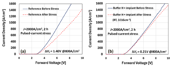
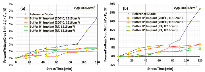
In terms of parameter optimization, a higher dose (1×10¹⁶ vs. 1×10¹⁵cm⁻²) and room-temperature implantation (vs. 200°C heated implantation) exhibited stronger suppression effects, attributed to more abundant point defects (hydrogen impurities, vacancies, and interstitials) that hinder dislocation glide. In addition, TCAD simulations confirmed that the hole concentration in the buffer layer after proton implantation was significantly below the threshold, proving that recombination centers effectively reduced the flux of injected holes.
3.3 Annealing Recovery and Synergistic Effect with Proton Implantation
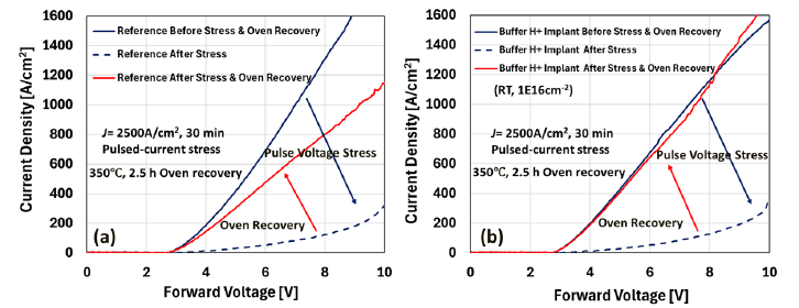
Notably, proton implantation not only suppresses degradation but also promotes recovery after degradation. After aging devices under high stress (2500A/cm²) and then annealing at 350°C in vacuum for 2.5 hours, the proton-implanted devices exhibited complete VF recovery, whereas the reference devices recovered only about half. This indicates that proton implantation modifies the crystalline environment of SFs, making them more prone to shrink back to the initial BPD state, possibly due to the modulation of dislocation migration energy by hydrogen-related defects. This finding provides a non‑destructive repair method for extending device lifetime.
References:
1. Fukaya, S., Yonezawa, Y., Kato, T., & Kato, M. (2022). Depth distribution of defects in SiC PiN diodes formed using ion implantation or epitaxial growth. physica status solidi (b), 259(9), 2100419.
2. Shimbori, A., Wada, R., Tokoro, N., Kuroi, T., Wong, H. Y., & Huang, A. Q. (2025). Suppression and Analysis of Bipolar Degradation in 4H-SiC PiN Diodes through Proton Implantation. Solid State Phenomena, 375, 69-75.
Discuss a substrate requirement with our team
Power Wafertech supplies 4H-SiC and other advanced semiconductor wafers tailored to your device specifications. Reach out to explore epitaxy and substrate solutions for your next project.
Contact Our Team