

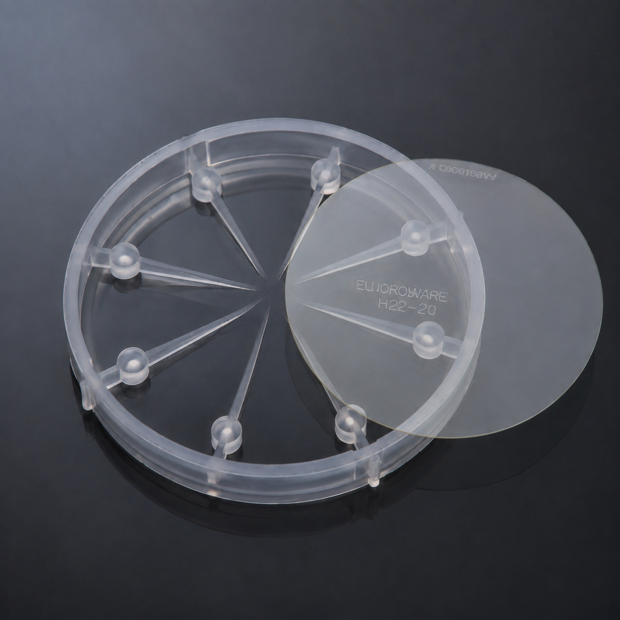
β-phase gallium oxide (β-Ga₂O₃) features an ultra-wide bandgap of approximately 4.9 eV, a high breakdown electric field, and outstanding radiation resistance. These properties enable it to maintain excellent performance in harsh radiation environments, demonstrating great application potential in aerospace, nuclear industry, and other fields. Power Wafertech Group supplies β-Ga₂O₃ substrates with orientations of (100), (010), (001), and (201). Detailed specifications are as follows:
1. Beta Gallium Oxide Substrate Specifications
| Item | Orientation | Size (mm) | Thickness (mm) | Resistivity UID (Ω·cm) | Resistivity Sn (Ω·cm) | Resistivity Mg/Fe (Ω·cm) | Flat | FWHM of DCRC (arc sec) | Dislocation Density (cm⁻²) | Surface Finished (nm) | Orientation Deviation |
|---|---|---|---|---|---|---|---|---|---|---|---|
| Square β-Ga₂O₃ | (100) | 10 ± 0.2 × 10.5 ± 0.2 | 0.5 (± 0.02) | 0.1~0.9 | 0.01~0.07 | ≥10¹⁰ | Long edge along [010] direction | ≤150 | <1 × 10⁵ | SSP/DSP; Ra < 0.5 | <±1° |
| (010) | 10 ± 0.2 × 10.5 ± 0.2 | 0.5 (± 0.02) | 0.1~0.9 | 0.01~0.07 | ≥10⁸ | Long edge along [010] direction | ≤150 | <1 × 10⁵ | SSP/DSP; Ra < 0.5 | <±1° | |
| (010) | 20 ± 0.2 × 21 ± 0.2 | 0.5 (± 0.02) | 0.1~0.9 | / | ≥10⁸ | Long edge along [010] direction | ≤150 | <1 × 10⁵ | SSP/DSP; Ra < 0.5 | <±1° | |
| (001) | 10 ± 0.2 × 10.5 ± 0.2 | 0.5 (± 0.02) | 0.1~0.9 | 0.01~0.07 | ≥10⁸ | Long edge along [010] direction | ≤250 | <1 × 10⁵ | SSP/DSP; Ra < 0.5 | <±1° | |
| (201) | 10 ± 0.2 × 10.5 ± 0.2 | 0.5 (± 0.02) | / | 0.01~0.07 | / | Long edge along [010] direction | ≤150 | <1 × 10⁵ | SSP/DSP; Ra < 0.5 | <±1° | |
| Round β-Ga₂O₃ | (100) | 50.8 ± 0.5 | 0.5 ± 0.02 | 0.1~0.9 | / | ≥10⁸ | [010] direction | ≤150 | <1 × 10⁵ | SSP/DSP; Ra < 0.5 | <±1° |
| (100) | 100 ± 0.5 | 0.5 ± 0.02 | 0.1~0.9 | 0.01~0.07 | ≥10¹⁰ | [010] direction | ≤150 | <1 × 10⁵ | SSP/DSP; Ra < 0.5 | <±1° | |
| (100) | 150 ± 0.5 | 0.8 ± 0.02 | 0.1~0.9 | 0.01~0.07 | / | [010] direction | ≤200 | <1 × 10⁵ | SSP/DSP; Ra < 0.5 | <±1° |
2. Ga₂O₃ Phase Stability and Crystal Structure
Gallium oxide has five allotropes: α, β, γ, δ, and ε, among which β-Ga₂O₃ is the most thermodynamically stable. When heated to sufficiently high temperatures, all other metastable phases transform into the β phase, which is the exclusive phase at the melting point (~1800°C). The formation free energies of different phases satisfy: β < ε < α < δ < γ. Under high-energy and high-pressure conditions, the β phase can transform into other metastable polymorphs; conversely, annealing metastable phases in air at 500–700°C yields stable β-Ga₂O₃. Currently, industrial production is dominated by the β phase of gallium oxide.
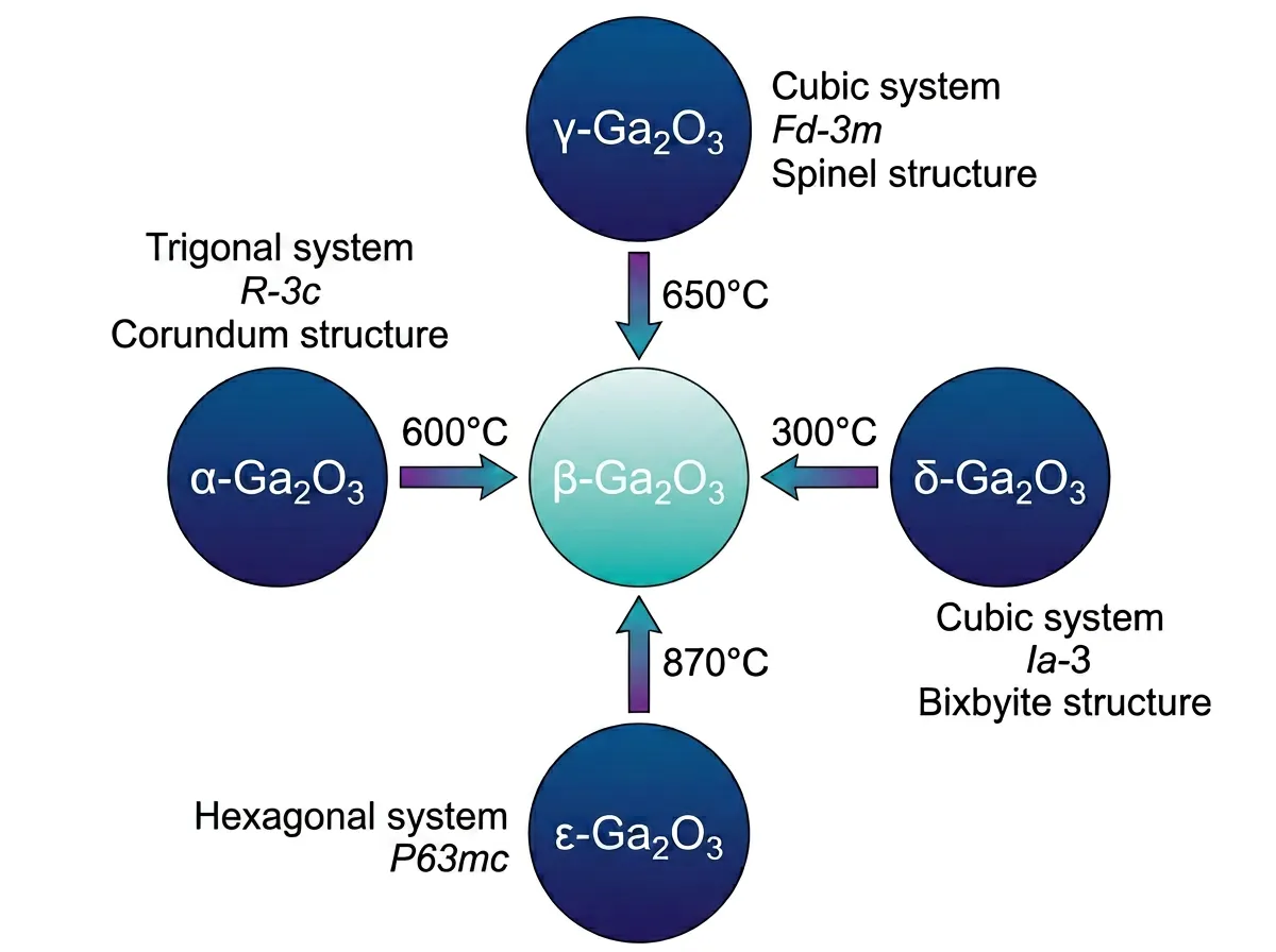
Fig. 1 — Ga₂O₃ phase transition diagram.
β-Ga₂O₃ is the only Ga₂O₃ phase that can be mass-produced efficiently and at low cost via melt-growth methods. Its crystal structure is monoclinic, space group C2/m, with lattice constants: a = 12.23(2) Å, b = 3.04(1) Å, c = 5.80(1) Å, α = γ = 90°, β = 103.7(3)°. Each unit cell contains two inequivalent Ga sites (GaⅠ, GaⅡ) and three inequivalent O sites (OⅠ, OⅡ, OⅢ). GaⅠ resides in a slightly distorted tetrahedral coordination environment bonded to four oxygen atoms; GaⅡ is in a highly distorted octahedral environment bonded to six oxygen atoms. OⅠ and OⅡ are both three-coordinated: OⅠ bonds with two GaⅠ and one GaⅡ, while OⅡ bonds with three GaⅡ. OⅢ is four-coordinated, bonding with two GaⅠ and two GaⅡ. This distorted lattice structure not only endows β-Ga₂O₃ substrate with high thermodynamic stability and excellent mechanical strength but also leads to significant anisotropy in surface energy, thermal conductivity, and carrier mobility across different crystallographic planes.
3. Single Crystal Growth Techniques for Gallium Oxide
Approximately 50% of the cost of Ga₂O₃ semiconductor products comes from substrate manufacturing, and the key to substrate fabrication lies in the choice of single crystal growth method. The main existing growth methods include edge-defined film-fed growth (EFG), Czochralski (CZ), vertical Bridgman (VB), floating zone (FZ), Verneuil, casting, and oxide crystal growth from cold crucible (OCCC). Each method has its advantages and disadvantages, but only EFG has been industrialized. Table 1 compares the technical characteristics of several major growth methods.
Table 1. Comparison of main β-Ga₂O₃ single crystal growth methods
| Growth Method | Max. Crystal Size | Growth Direction | Atmosphere | Crucible | Key Advantages | Main Limitations |
|---|---|---|---|---|---|---|
| CZ | 2 inch | [010] | Limited O₂ | Iridium | Mature process, easy scaling; controllable doping concentration; suitable for mass production. | Melt-crystal interface prone to distortion, limiting diameter expansion beyond 6 inches. |
| EFG | 6 inch | [010] | Limited O₂ | Iridium | Ir die provides stable thermal field; can grow 6-inch crystal ribbons with complex cross-sections; high growth rate (5–10 mm/h). | Heavy reliance on expensive Ir crucibles; high equipment investment and operating costs. |
| OFZ | 1 inch | Various orientations | Various O₂ | Crucible-free | No crucible to avoid contamination from foreign metals; extremely high crystal purity, low dislocation density. | Diameter typically ≤1 inch; requires stable growth in high vacuum or high-purity O₂/Ar atmosphere. |
| VB | 6 inch | Various orientations | Air | Pt-30%Rh | Can grow directly in air (Pt-Rh/Ir crucible); good crystal isotropy; scalable to 6 inches. | Rh/Ir dissolution contamination; narrow windows for temperature gradient and pull rate. |
| OCCC | 2 inch | [010] | Air | Copper | Water-cooled copper crucible replaces precious metal crucibles, cost reduced by ~40%; frequency adjustable to achieve CZ-like thermal field and interface shape; high crystal purity. | Unstable melt convection; difficult to prepare electrically insulating crystals; deep crucible (>50 mm) design poses stability challenges. |
4. β-Ga₂O₃ Substrate Processing Challenges
High-precision, low-damage substrates are the foundation of high-performance devices. β-Ga₂O₃ is a typical difficult-to-machine material due to its strong chemical inertness, hardness and brittleness, significant anisotropy, and pronounced cleavage characteristics. Mechanical behaviors vary markedly across different crystal planes: under the same load, the damage depth on the (001) plane is approximately twice that on the (100) plane; the nanoindentation cutting depth ranges on the (010) and (100) planes are 96.5–576.8 nm and 84.6–421.6 nm, respectively. Micro-pillar compression tests also confirm significant differences in fracture stress and strain among the (200), (001), and (010) planes.
These characteristics lead to problems such as brittle flaking, crack propagation, and low polishing rates during processing. Studies indicate that the direction 105° within the (010) plane of Ga₂O₃ is the most machinable orientation, offering more stable material removal and less damage; therefore, the (010) plane is recommended as the preferred processing surface. Developing orientation-specific processes and adapting chemical mechanical polishing (CMP) systems are key to achieving high-quality β-Ga₂O₃ wafer fabrication.
5. Beta Ga₂O₃ Wafer Applications
Based on the above material properties and substrate processing capabilities, β-Ga₂O₃ demonstrates unique advantages in several optoelectronic device areas.
5.1 Deep-UV Photodetection
The cutoff wavelength of β-Ga₂O₃ lies in the deep-ultraviolet (DUV) region of 250–280 nm, with virtually no response to visible and infrared light, thus enabling highly selective, low-background-noise DUV detection.
5.2 Nuclear Radiation Detection
β-Ga₂O₃ has a high density of 6.44 g·cm⁻³ and excellent scintillation properties, allowing efficient detection of α, β, γ particles and neutron radiation. It maintains long-term stable operation under high-dose radiation environments and exhibits strong radiation damage resistance.
5.3 Additional Applications
Furthermore, β-Ga₂O₃ possesses outstanding mechanical strength and chemical corrosion resistance, making it promising for high-temperature sensing, corrosion-resistant photonic devices, and extreme-environment electronics.
Discuss a β-Ga₂O₃ substrate requirement with our team
Power Wafertech supplies high-quality β-Ga₂O₃ substrates and epitaxial solutions tailored to your device specifications. Reach out to explore orientations, doping types, and wafer geometry options for your next project.
Contact Our Team