

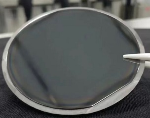
Indium phosphide (InP)-based high electron mobility transistors (HEMTs) are widely used in demanding high-frequency applications, particularly where low noise and high electron transport performance are essential. They are especially relevant to cryogenic low-noise amplifiers (LNAs) for radio astronomy, quantum computing readout, and millimeter-wave and submillimeter-wave systems.
The performance of an InP HEMT depends not only on gate length, contact resistance, and device processing, but also on the underlying epitaxial structure. The InGaAs channel, InAlAs barrier, spacer layer, and doping profile collectively determine the two-dimensional electron gas (2DEG), influencing carrier mobility, threshold voltage, noise performance, and fabrication compatibility.
For device developers, optimizing InP HEMT epitaxy requires balancing electron transport, electrostatic control, and process integration. This article examines two important considerations: spacer-layer engineering for cryogenic low-noise performance and cap-layer stability during device fabrication.
1. InP HEMT Epitaxial Structures
InP HEMT epitaxial wafers commonly employ an InGaAs channel and an InAlAs barrier grown on a semi-insulating InP substrate. The lattice-matched heterostructure supports high-mobility electron transport, while the doping profile and spacer design help control electron transfer and 2DEG formation.
Depending on device requirements, the epitaxial stack may include an InGaAs cap layer, an InP etch-stop layer, an InAlAs barrier, a spacer layer, an InGaAs channel, and an InAlAs buffer.
Two representative structures are outlined below. Exact thicknesses and doping concentrations depend on the intended device architecture and should be established through project-specific design.
1.1 Delta-Doped InGaAs/InAlAs/InP HEMT
A delta-doped structure uses a thin, highly localized doping plane to supply electrons to the channel. An undoped spacer separates the dopants from the InGaAs quantum well, helping reduce ionized-impurity scattering while maintaining a high carrier concentration.
| Epi-Layer | Material | Thickness | Dopant |
|---|---|---|---|
| Cap | InGaAs | * | * |
| Etch stop | InP | * | * |
| Barrier | InAlAs | * | * |
| Planar doping | * | * | |
| Spacer | InAlAs | 5nm | * |
| Channel | InGaAs | * | * |
| Buffer | InAlAs | * | * |
| Substrate | SI-InP |
The delta-doping concentration and spacer thickness must be optimized together. Excessively close proximity between the dopants and channel can increase impurity scattering, while an excessively thick spacer may change electron transfer and the electrostatic characteristics of the device.
1.2 InGaAs/InAlAs/InP HEMT for Low-Noise Applications
Low-noise InP HEMTs use a similar heterostructure, with the layer sequence and doping profile tailored to the target operating temperature, frequency range, and noise requirements. A representative structure as:
| Epi-Layer | Material | Thickness | Dopant |
|---|---|---|---|
| Cap | InGaAs | 20nm | * |
| Etch stop | InP | * | * |
| Barrier | InAlAs | * | * |
| Spacer | InAlAs | * | * |
| Channel | InGaAs | * | * |
| Buffer | InAlAs | * | * |
| Substrate | SI-InP |
For cryogenic LNAs, epitaxial design should account for low-temperature carrier mobility, threshold voltage, gate control, and intrinsic channel noise. For millimeter-wave devices, the relevant trade-offs may also include carrier density, access resistance, parasitic capacitance, and high-frequency gain.
PWG can discuss customized InP-based epitaxial growth requirements according to the target layer sequence, thicknesses, doping profiles, and substrate specifications.
2. Spacer-Layer Thickness and Cryogenic Noise Performance
In a typical InP HEMT, electrons supplied by a Si delta-doped layer transfer into the InGaAs quantum well, forming a 2DEG near the InAlAs/InGaAs heterointerface. The undoped InAlAs region between the dopant plane and the channel is known as the spacer layer.
Spacer thickness, commonly denoted as dSP, influences the balance between carrier concentration, mobility, and electrostatic control. A thinner spacer places the ionized dopants closer to the channel, potentially increasing impurity scattering. Increasing the spacer thickness can improve mobility, but the optimum value depends on the complete heterostructure and device operating conditions.
2.1 Influence on Mobility and DC Characteristics
Li et al. (2022) investigated InP HEMTs with spacer thicknesses of 1, 3, 5, and 7 nm. The delta-doping concentrations were calibrated to maintain a surface electron concentration of approximately 2.5 × 1012 cm−2.
At low temperature, the reported Hall mobility increased from approximately 17,000 cm²/V·s for the 1 nm spacer to 53,000 cm²/V·s for the 5 nm spacer, with further improvement approaching saturation at 7 nm.
The results indicate that a very thin spacer can increase impurity scattering and limit electron transport. However, maximizing mobility alone does not necessarily produce the best overall device performance.
At 5 K, the 1 nm spacer device showed reduced current-driving capability. The 5 nm spacer device achieved a subthreshold swing of approximately 12 mV/dec and a threshold voltage of 0.1 V, demonstrating favorable gate control under the reported test conditions.
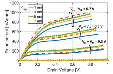
Fig. 1 — Output characteristics of InP HEMTs with different spacer-layer thicknesses
2.2 Spacer Thickness and Low-Temperature Noise
To evaluate the practical impact on noise, the researchers integrated HEMTs with different spacer thicknesses into three-stage LNAs operating over 4–8 GHz and measured their noise temperatures at 5 K.
The average measured LNA noise temperatures were:
| Spacer thickness | Average LNA noise temperature |
|---|---|
| 1 nm | 1.9 K |
| 3 nm | 1.7 K |
| 5 nm | 1.4 K |
| 7 nm | 1.6 K |
Among the tested structures, the 5 nm spacer delivered the lowest average noise temperature. The extracted drain noise temperature also reached its minimum for this structure, indicating lower intrinsic channel noise under the investigated operating conditions.
These results demonstrate that spacer-layer optimization can directly influence the low-temperature noise performance of InP HEMTs. They also show why epitaxial design should be evaluated against device-level operating requirements rather than carrier mobility alone.
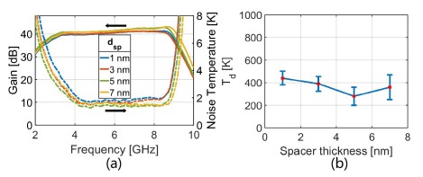
Fig. 2 — Gain and noise temperature of cryogenic LNAs incorporating InP HEMTs with different spacer thicknesses, including extracted drain noise temperature
2.3 Real-Space Transfer and the Optimum Spacer Thickness
One mechanism discussed by Li et al. is real-space transfer (RST), in which energetic channel electrons cross the potential barrier and enter the barrier layer. This process can introduce additional noise and reduce the efficiency of the intended channel transport.
In the reported study, devices with 1 and 3 nm spacers exhibited negative differential resistance under high gate voltage, whereas the 5 and 7 nm devices did not show the same behavior under the tested conditions.
The researchers also found that the 5 nm spacer structure had the lowest gate overdrive voltage at the optimum noise bias. This was consistent with reduced real-space transfer and the lower measured noise temperature.
The findings highlight the interaction between spacer thickness, threshold voltage, carrier transport, and noise generation. For cryogenic InP HEMTs, the optimum spacer is therefore a device-specific design parameter rather than a fixed value applicable to every epitaxial structure.
3. Cap-Layer Stability and Contact Resistance in InP HEMT Processing
Electrical performance is only one part of successful InP HEMT epitaxy. The cap layer must also remain compatible with subsequent metallization, resist removal, and other fabrication steps.
Saranovac et al. (2019) investigated electrochemical etching in InP HEMT fabrication and reported that moisture contamination during metal lift-off could damage highly doped GaInAs/InGaAs-based cap structures, depending on the material system and processing conditions.
Such damage can reduce the effective contact area and increase ohmic contact resistance, undermining the electrical benefits of an otherwise well-designed epitaxial structure.
3.1 Moisture-Related Etching During Metal Lift-Off
In the reported experiments, contact resistance increased with increasing water content in the N-methyl-2-pyrrolidone (NMP) lift-off solvent and with longer exposure times.
Cross-sectional and surface SEM observations revealed lateral etching beneath metal edges, creating voids in the cap layer and reducing the effective contact area.
These results indicate that cap-layer integrity can be affected by interactions between the semiconductor, metal, and processing environment. Moisture control and lift-off conditions therefore deserve attention when developing reliable InP HEMT fabrication processes.
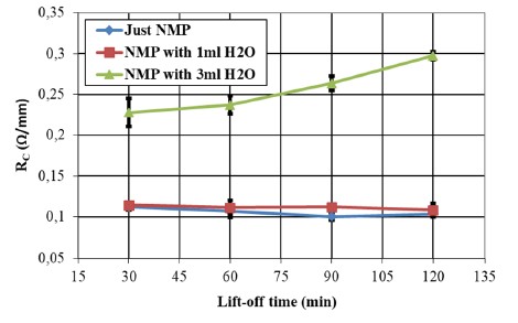
Fig. 3 — Variation trend of contact resistance under different water contents and lift-off times
3.2 Relationship Between Doping and Electrochemical Etching
The study proposed that moisture-related solvent chemistry and electrochemical reactions between the metal and semiconductor contributed to the observed cap-layer damage.
Highly doped cap layers can provide a low-resistance path for ohmic contact formation, but their behavior during wet processing must also be considered. Under the investigated conditions, higher doping was associated with more severe etching, illustrating a potential trade-off between contact resistance and process stability.
The implications are important for epitaxial design: increasing cap-layer doping should not be treated as an isolated solution to contact resistance. The selected material composition, doping profile, metal system, and fabrication environment must be considered together.
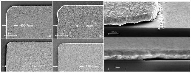
Fig. 4 — SEM images showing lateral etching and void formation beneath metal contacts during lift-off processing
These observations do not mean that highly doped cap layers are inherently unsuitable. Rather, they emphasize the need to match epitaxial specifications with the intended fabrication process and to control moisture exposure during sensitive processing steps.
4. Key Considerations for InP HEMT Epitaxial Design
The performance of InP HEMTs depends on the interaction between epitaxial structure, carrier transport, and fabrication conditions. The studies discussed above highlight several important considerations:
- 2DEG engineering: Channel composition, barrier structure, and doping profile influence carrier concentration and confinement.
- Spacer-layer optimization: Spacer thickness affects impurity scattering, electron mobility, threshold voltage, and cryogenic noise performance.
- Low-temperature operation: Epitaxial parameters should be evaluated against the target operating temperature, frequency range, and noise requirements.
- Cap-layer stability: Cap composition and doping must be considered alongside metallization, contact resistance, and lift-off conditions.
- Process compatibility: Epitaxial design and fabrication processes should be optimized together to balance electrical performance and manufacturing reliability.
There is no single epitaxial structure that is optimal for every InP HEMT application. The appropriate combination of layer thicknesses, doping profiles, and material compositions depends on the intended device architecture and operating conditions. Careful epitaxial design is therefore essential for achieving the required balance between low noise, high electron mobility, electrostatic control, and process compatibility.
References
- Li, J., Pourkabirian, A., Bergsten, J., Wadefalk, N., & Grahn, J. (2022). Influence of spacer thickness on the noise performance in InP HEMTs for cryogenic LNAs. IEEE Electron Device Letters, 43(7), 1029–1032.
- Saranovac, T., Ruiz, D. C., Han, D., Arabhavi, A. M., Ostinelli, O., & Bolognesi, C. R. (2019). Effects of electrochemical etching on InP HEMT fabrication. IEEE Transactions on Semiconductor Manufacturing, 32(4), 496–501.
Discuss an InP HEMT epitaxy with our team
Power Wafertech supplies customized semiconductor epitaxial materials for high-frequency and low-noise device applications. Reach out to explore InP HEMT epitaxial structures aligned with your device architecture and process requirements.
Contact Our Team