


The constraints on AI infrastructure are no longer defined only by how many accelerators can be manufactured. They are increasingly defined by how much power can be delivered, converted, and dissipated inside a rack. That shift has quietly turned power conversion into one of the most consequential semiconductor markets of the decade, and it is redrawing the boundary between silicon carbide and gallium nitride in ways that matter to anyone specifying substrates or epitaxial wafers.
This article maps where each material sits in the emerging architecture, why the split is happening, and what it implies for material specifications through the rest of the decade.
1. The rack power problem: from 10 kW to over 100 kW
Conventional enterprise racks were designed around power levels of roughly 6–10 kW. AI training racks routinely exceed 50 kW today, and deployments approaching or surpassing 100 kW per rack are being built. At those densities, every percentage point of conversion loss becomes heat that must be removed, and every cubic centimetre occupied by magnetics and heatsinks is space not occupied by compute.
Traditional silicon-based power conversion stages struggle to exceed roughly 90% efficiency in these conditions. The gap between 90% and 98% sounds small; at 100 kW per rack it is the difference between 8 kW and 2 kW of waste heat per rack, multiplied across thousands of racks. That arithmetic is the entire business case for wide bandgap adoption in data centers.
2. Why 800 V DC, and why now
As rack power rises, the current required at conventional distribution voltages becomes impractical: cable cross-sections, connector ratings, and resistive losses all scale with current. Moving the distribution bus to 800 V DC reduces current proportionally, cutting distribution losses substantially and reducing copper volume.
The 800 V HVDC architecture is being adopted in parallel with two related developments: solid-state transformers (SST) that handle medium-voltage AC to 800 V DC conversion in a single stage, and a move toward single-stage AC-DC conversion at the rack. Both push semiconductor devices toward higher blocking voltages and higher switching frequencies simultaneously — a combination that silicon cannot satisfy.
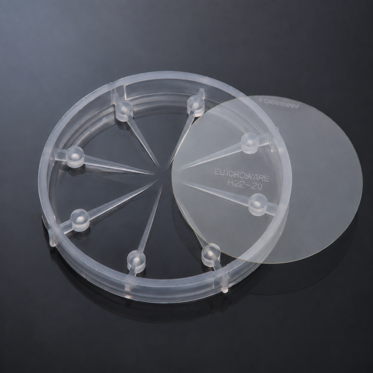
Fig. 1 — GaN HEMT epitaxial wafer. GaN's high electron mobility and low switching loss make it the default choice for high-frequency intermediate bus conversion.
3. SiC takes the high-voltage front end
In an 800 V architecture, the grid-facing stages — rectification, power factor correction, and the interface to medium-voltage distribution — operate at voltages and power levels where SiC MOSFETs are the practical choice. SiC devices in these positions reach efficiencies above 97% while operating at temperatures and power densities that silicon IGBTs cannot sustain. The same devices also serve the uninterruptible power supplies and storage converters that sit alongside the compute load.
For medium-voltage and solid-state transformer applications, the voltage requirement rises into the 3.3 kV class and above. This is a structurally important segment because it favours device qualification over unit cost, and because the epitaxial structures involved — thick drift layers with tightly controlled doping — are among the most demanding in volume SiC production.
4. GaN owns the last inch: 48 V to 12 V and below
Once the bus is at 800 V or 48 V, the remaining conversion happens close to the load, at voltages where switching frequency — not blocking voltage — determines performance. This is where GaN HEMTs dominate. Operating LLC resonant and similar topologies at 500 kHz to 1 MHz, GaN enables efficiencies above 98% while shrinking transformers, inductors, and capacitors, which is what allows server supply power density to rise by roughly 30% without a corresponding rise in cooling demand.
The economics of this transition depend on GaN-on-Si. Growing GaN epitaxy on silicon substrates allows the use of established, low-cost silicon fabrication infrastructure, and the shift from 6-inch to 8-inch GaN-on-Si has been reported to reduce unit cost by roughly 30%. That cost step is what moves GaN from a premium option in consumer fast chargers to a default choice in server power.
The observable trend: reported GaN device counts per rack have risen from roughly a dozen units in 2024 to close to forty by 2026 as intermediate bus conversion stages proliferate. Growth in this metric tracks AI server deployment more closely than any other wide bandgap indicator.
5. Specification map: where each material sits
| Conversion stage | Typical voltage | Dominant device | Material basis | Dominant specification driver |
|---|---|---|---|---|
| Medium-voltage AC to DC (SST, utility interface) | kV class | High-voltage SiC MOSFET / module | SiC epi on SiC substrate | Thick drift layer uniformity, blocking voltage, reliability under high field |
| 800 V input rectification and PFC | 800 V | 1200 V–1700 V SiC MOSFET | SiC epi on SiC substrate | On-resistance, switching loss, high-temperature stability |
| 800 V to 48 V / 50 V intermediate conversion | 800 V → 48–50 V | GaN HEMT (bidirectional where applicable) | GaN-on-Si epi | Dynamic on-resistance, switching frequency, thermal resistance |
| 48 V to 12 V bus conversion | 48 V → 12 V | GaN HEMT / integrated GaN power IC | GaN-on-Si epi | Switching loss, integration density, package parasitics |
| Point-of-load near the accelerator | 12 V and below | GaN power stage / Si driver | GaN-on-Si epi | Transient response, current density |

Fig. 2 — SiC epitaxial wafer. High-voltage front-end stages in 800 V architectures depend on thick, uniform drift layers.
6. What this means for substrate and epitaxy buyers
Two specification trends follow directly from this architecture split, and both are already visible in qualification requests.
6.1 SiC: thickness and uniformity, not just resistivity
As designs move toward 1200 V and 1700 V platforms — and toward 3.3 kV for grid-adjacent equipment — epitaxial thickness and doping uniformity become yield-limiting. Buyers specifying SiC epi for these applications should define within-wafer thickness tolerance, doping concentration tolerance, and defect density limits explicitly, and should require batch-level verification rather than typical values.
6.2 GaN: dynamic behaviour and wafer-level uniformity
For GaN HEMTs, the specification conversation has moved beyond static on-resistance. Dynamic on-resistance behaviour, current collapse, and threshold voltage stability under thermal and electrical stress are now central, and all of them trace back to epitaxial quality: buffer design, trap density, barrier composition and thickness, and interface roughness. In ultrathin-barrier InAlN/GaN structures used for high-frequency and millimeter-wave operation, barrier thickness control at the nanometre scale and suppression of phase separation are the determining factors.
Practically, this means GaN epi buyers should request sheet resistance mapping, 2DEG mobility and density data, and evidence of wafer-to-wafer repeatability — not just a nominal structure diagram.
7. Beyond the hyperscalers: where the spillover lands
The wide bandgap capacity, process know-how, and qualification data generated by AI power programs do not stay confined to data centers. Three adjacent markets are absorbing the spillover:
- Stationary storage and grid infrastructure. The same high-voltage SiC devices developed for 800 V DC distribution apply directly to storage converters and grid-forming inverters, where efficiency and thermal behaviour determine total cost of ownership.
- Electric vehicle powertrains. Higher-voltage vehicle platforms benefit directly from the cost reductions achieved when 8-inch capacity is built out for data center demand, even though automotive qualification timelines remain substantially longer.
- Optoelectronics and sensing. The photonics and optical links that connect AI clusters draw on the same GaN materials platform as power devices: laser diodes, photodetectors, and UV sensing structures share epitaxial infrastructure and much of the underlying process knowledge.
8. The takeaway for 2026 planning
The cleanest way to read this market is as a division of labour rather than a competition between materials. SiC wins where voltage is high and switching frequency is moderate; GaN wins where frequency is high and voltage is moderate; silicon retains the cost-sensitive and control functions where neither matters. The rack is not choosing between them — it is using all three, in increasing quantities, in the same power chain.
For material buyers, the risk in 2026 is not choosing the wrong material. It is specifying that material too loosely to move between suppliers when allocation tightens. Architectures are converging, which means the differentiation is increasingly in epitaxial consistency — and consistency is something that has to be specified before it can be purchased.
9. How PWG supports wide bandgap power programs
Power Wafertech Group supplies SiC substrates and epitaxial wafers, GaN epitaxial structures on sapphire, silicon, SiC, and freestanding GaN substrates, and related wide bandgap materials for both power and optoelectronic applications. For teams qualifying 800 V front-end designs, the relevant support is epitaxial structure design against a target blocking voltage, with documented thickness and doping uniformity. For GaN programs, it is barrier and buffer engineering aimed at the dynamic performance metrics described above, backed by wafer-level electrical mapping.
Data sources
- SEMI and SEMI Silicon Manufacturers Group, quarterly shipment and market statistics.
- SEMI 300 mm fab equipment spending forecasts and AI-investment commentary.
- SUMCO and industry analyses on AI-related silicon and wafer demand intensity.
- Published power-electronics architecture work on 800 V HVDC, solid-state transformers, and single-stage AC-DC conversion presented at industry conferences including APEC 2026.
- Market research on GaN power device adoption in data center, automotive, and consumer applications; market size estimates differ substantially between research houses and are presented here as directional trends rather than precise figures.
- Device count and cost reduction figures cited for GaN-on-Si are industry estimates reported across multiple sources.
Discuss a substrate requirement with our team
Power Wafertech supplies high-quality semiconductor wafers and epitaxial solutions tailored to your device specifications. Reach out to explore substrate and epiwafer options for your next project.
Contact Our Team