
SiC Substrate | 4H, 6H, 3C | Power Wafertech Group

SiC Wafers

SiC Substrate

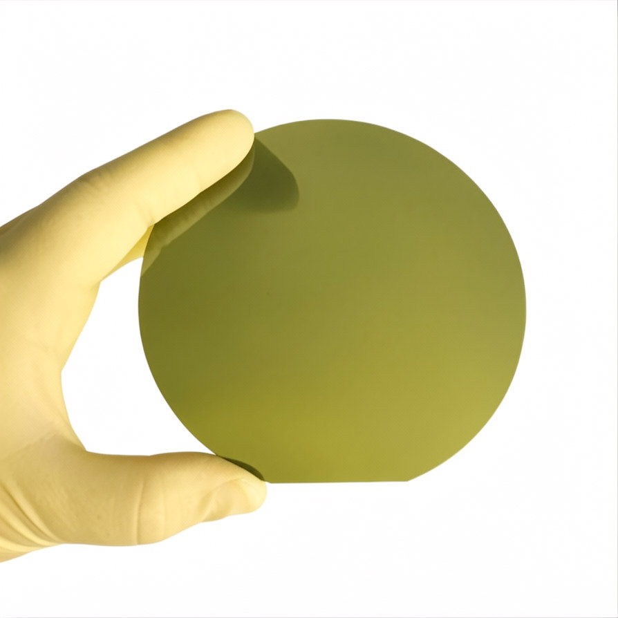
Premium SiC substrate wafers for power, RF, and optoelectronic devices. Available in 4H, 6H, and 3C polytypes with N-type, P-type, and semi-insulating options. Offered in 2"–12" sizes with Epi-ready finishes for advanced semiconductor fabrication.
  • Polytypes — 4H-SiC · 6H-SiC · 3C-SiC
  • Conductivity — N-type · P-type · Semi-insulating
  • Doping Options — N-doped · Al-doped · V-doped
  • Sizes — 2″ · 3″ · 4″ · 6″· 8″· 12″
  • Surface — SSP · DSP ·Epi-ready
  • Packaging — Single wafer cassette, vacuum sealed
Detailed Specifications

Specifications by wafer type.

Select a wafer type to view detailed specs

Parameter 8”/200mm 4H-SiC Substrate
Polytype 4H
Diameter 200±0.2mm
Thickness 350±25µm, 500±25µm
Orientation 4° toward (11-20) ±0.5°
Conduction Type N type
Dopant Nitrogen (N)
Resistivity 0.015~0.03Ω·cm
MPD ≤2ea/cm² (A grade); ≤10ea/cm² (B grade); ≤50ea/cm² (C grade)
TTV ≤10µm(A grade); ≤15µm (B grade); ≤20µm (C grade)
Bow -25~25µm(A grade); -45~45µm(B grade); -65~65µm(C grade)
Warp ≤35µm(A grade); ≤50µm (B grade); ≤70µm (C grade)
Surface Roughness Si-face CMP Ra ≤0.2nm; C-face optical polish <5nm
Surface Finish SSP / DSP, epi-ready
Packaging Single or multi‑wafer cassette, vacuum sealed
Applications

Where this wafer delivers value

01

Power Electronics

SiC substrates deliver high breakdown voltage and low switching losses, enabling high-efficiency power devices. Typical devices: SiC MOSFETs, Schottky Barrier Diodes (SBDs), and IGBTs. Applications: EV powertrains, fast charging, smart grids, industrial motor drives.
02

RF & Microwave Devices

Semi-insulating 4H-SiC is the preferred platform for GaN-on-SiC HEMTs. Its excellent thermal conductivity ensures high-frequency performance. Applications: 5G/6G base stations, radar systems, satellite communications.

03

Emerging AR/MR Applications

High refractive index and excellent optical properties. Ideal for photonic integrated circuits (PICs) and optical waveguides, enabling compact, high-efficiency AR/MR displays.

04

Extreme-Environment Electronics

High-temperature resistance and radiation hardness (rad-hard). Engineered for harsh environments: aerospace systems, deep-well drilling sensors, nuclear instrumentation, and critical defense electronics.

FAQ

Common questions about this product

Quick answers on material selection, customization, testing and ordering.

PWG provides high-quality SiC substrates in 4H, 6H, and 3C polytypes. We offer N-type (N-doped), P-type (Al-doped), and semi-insulating (V-doped) wafers with epi-ready surface finishes to meet your specific device requirements.

N-type SiC: Typically nitrogen-doped, widely used for SiC power devices and epitaxial growth. P-type SiC: Typically aluminum-doped, suitable for PN junctions, bipolar devices, and specialized device structures. Semi-insulating SiC: Typically vanadium-doped, designed for high-frequency applications, particularly as a substrate for GaN HEMT epitaxy.

Our SiC substrates are available with different micropipe density (MPD) grades depending on wafer size. For selected 4H-SiC substrates, MPD can be as low as ≤0.1 cm⁻², while 6" and 8" products are available with specifications tailored to your grade and application.

Yes. Beyond bare substrates, we support value-added processing including dicing, grinding, thinning, CMP polishing, backside metallization, crystal bonding, and ion implantation according to project requirements.

Technical Inquiry

Speak to Engineers About Your Wafer Needs

Share your material, dimensions, specifications, application or project stage. Our team will review your requirements and respond within one business day.

Engineering-led response

Inquiries are routed to the appropriate technical or commercial team.

Address

No. 1389, Lianmei Road, Lianhua Industrial Zone, Tong’an, Xiamen, Fujian 361100, China

File Upload
Emailvictorchan@powerwafertech.com Phone+86-592-5633652