
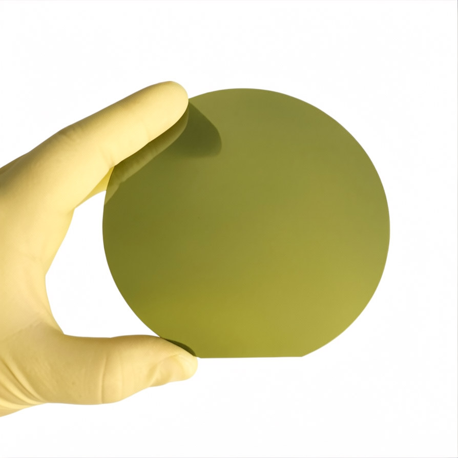
SiC Epitaxy
- Polytypes — 4H-SiC (homoepitaxy) / 3C-SiC (homo- & heteroepitaxy)
- Conductivity — N-type, P-type, Semi-insulating
- Diameters — 2″, 4″, 6″, 8″
- Thickness range — 0.5 – 200µm (customizable)
- Structure — Custom multilayer structures, buffer layers, and precise doping profiles
- Thick epitaxial layer — provides 30~200µm thick epitaxial growth service for ultra-high voltage devices, ensuring good uniformity and crystal quality.
Published specifications by wafer diameter.
Select a diameter to review the corresponding published specification set.
Common questions about this product
Quick answers on material selection, customization, testing and ordering.
For standard 4H-SiC homoepitaxy, carrier concentration can be controlled over approximately 1×10¹⁴–1×10¹⁹ cm⁻³, depending on the conductivity type and epi design.
For standard 4H-SiC homoepitaxy, thickness uniformity can be controlled to approximately ≤10%. For selected P-type SiC epi structures, uniformity can reach ≤4%. Actual performance depends on wafer size, epi thickness, and structure.
Yes. PWG can develop custom multilayer epitaxial structures, including buffer layers, current-spreading layers, channel layers, barrier layers, and other device-specific structures.
Yes. 30–200 μm thick SiC epitaxial layers can be developed for ultra-high-voltage applications. Thickness, doping concentration, and uniformity can be optimized according to the target breakdown voltage.
Technical Inquiry
Speak to Engineers About Your Wafer Needs
Share your material, dimensions, specifications, application or project stage. Our team will review your requirements and respond within one business day.
Engineering-led response
Inquiries are routed to the appropriate technical or commercial team.
Address
No. 1389, Lianmei Road, Lianhua Industrial Zone, Tong’an, Xiamen, Fujian 361100, China
Phone