01
Optical Communications & Photonics
Applications: DFB lasers, EMLs, PIN photodiodes, APDs for 1.3–1.55µm fiber-optic communications. Recommended Spec: N-type or Semi-insulating (Fe-doped) InP.

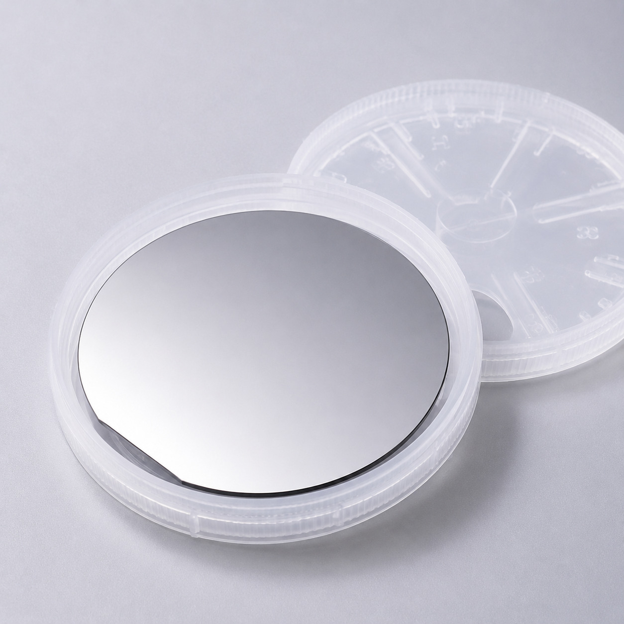
Select a wafer type to view detailed specs
Export of this product is regulated by the Ministry of Commerce of the PRC (MOFCOM). An export license must be obtained prior to shipment. Please contact our compliance team for details.
Export of this product is regulated by the Ministry of Commerce of the PRC (MOFCOM). An export license must be obtained prior to shipment. Please contact our compliance team for details.
Export of this product is regulated by the Ministry of Commerce of the PRC (MOFCOM). An export license must be obtained prior to shipment. Please contact our compliance team for details.
Export of this product is regulated by the Ministry of Commerce of the PRC (MOFCOM). An export license must be obtained prior to shipment. Please contact our compliance team for details.
Applications: DFB lasers, EMLs, PIN photodiodes, APDs for 1.3–1.55µm fiber-optic communications. Recommended Spec: N-type or Semi-insulating (Fe-doped) InP.
Applications: HBTs, HEMTs, HEMT MMICs, THz detectors and sources. Recommended Spec: Semi-insulating InP for RF/MMIC; Conductive InP for HBT/Hemt.
Applications: Optical transceivers, data-center interconnects, coherent communications. Recommended Spec: Semi-insulating or N-type InP based on device architecture.
Quick answers on material selection, customization, testing and ordering.
N-type (S-doped) and P-type (Zn-doped) are conductive substrates for optoelectronic and electronic devices. Semi-insulating (Fe-doped) InP features high resistivity and is ideal for RF, microwave, and high-frequency applications.
For 1.3–1.55µm DFB lasers, EMLs, and photodetectors, we recommend N-type or Semi-insulating (Fe-doped) InP wafer, depending on the specific epitaxial structure and device design.
Semi-insulating (Fe-doped) InP is primarily selected for RF, microwave, and THz devices due to its high resistivity and excellent electrical isolation.
Yes. We support R&D prototyping and small-batch orders. Custom orientations, doping, and epi-ready specifications are available upon request.
Wafers are packaged in vacuum-sealed single-wafer cassettes within an ISO-certified cleanroom. We ensure Fab-ready delivery with door-to-door shipping.
Technical Inquiry
Share your material, dimensions, specifications, application or project stage. Our team will review your requirements and respond within one business day.
Engineering-led response
Inquiries are routed to the appropriate technical or commercial team.
Address
No. 1389, Lianmei Road, Lianhua Industrial Zone, Tong’an, Xiamen, Fujian 361100, China
Phone