
01
Heavily Doped Si
Power devices, MOSFETs, IGBTs, power diodes, epitaxial substrates | Typical Resistivity: 0.0005–0.005 Ω·cm

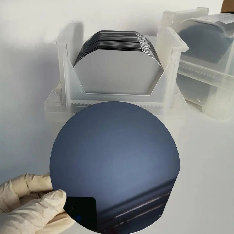
Select a wafer type to view detailed specs
Power devices, MOSFETs, IGBTs, power diodes, epitaxial substrates | Typical Resistivity: 0.0005–0.005 Ω·cm
ICs, CMOS, MEMS, sensors, semiconductor R&D | Typical Resistivity: 0.005–100 Ω·cm
RF devices, high-frequency circuits, sensors, research | Typical Resistivity: 100–10,000 Ω·cm
RF, microwave, detector and specialized research applications | Typical Resistivity: >10,000 Ω·cm
Quick answers on material selection, customization, testing and ordering.
Our silicon wafer portfolio covers approximately 0.0005 Ω·cm to >10,000 Ω·cm, depending on crystal growth method and doping requirements.
Yes. We supply prime, test, dummy and research-grade wafers according to the application and quality requirements.
Yes. Diameter, orientation, doping, resistivity, thickness, surface finish, TTV, bow and warp can be customized for specific device or process requirements.
Technical Inquiry
Share your material, dimensions, specifications, application or project stage. Our team will review your requirements and respond within one business day.
Engineering-led response
Inquiries are routed to the appropriate technical or commercial team.
Address
No. 1389, Lianmei Road, Lianhua Industrial Zone, Tong’an, Xiamen, Fujian 361100, China
Phone


