
01
MOS & Gate Dielectrics
Thin dry thermal SiO₂ layers can be used as gate dielectric or insulating layers in MOS-based device structures. MOSFETs MOS capacitors Analog devices Sensor devices Semiconductor R&D

Select a wafer type to view detailed specs
Thin dry thermal SiO₂ layers can be used as gate dielectric or insulating layers in MOS-based device structures. MOSFETs MOS capacitors Analog devices Sensor devices Semiconductor R&D
Thicker SiO₂ layers provide electrical insulation between device structures and can be used for isolation processes. Power ICs High-voltage devices RF devices Device isolation structures
Thermal oxide layers can function as insulation, masking or sacrificial layers in MEMS fabrication. MEMS sensors Pressure sensors Microstructures Silicon micromachining
SiO₂ provides a useful masking layer for selected semiconductor processing steps. Dopant diffusion Ion implantation processes Etching processes Device fabrication
Thermal oxide can also be used as a protective and insulating layer in silicon-based device structures.
Quick answers on material selection, customization, testing and ordering.
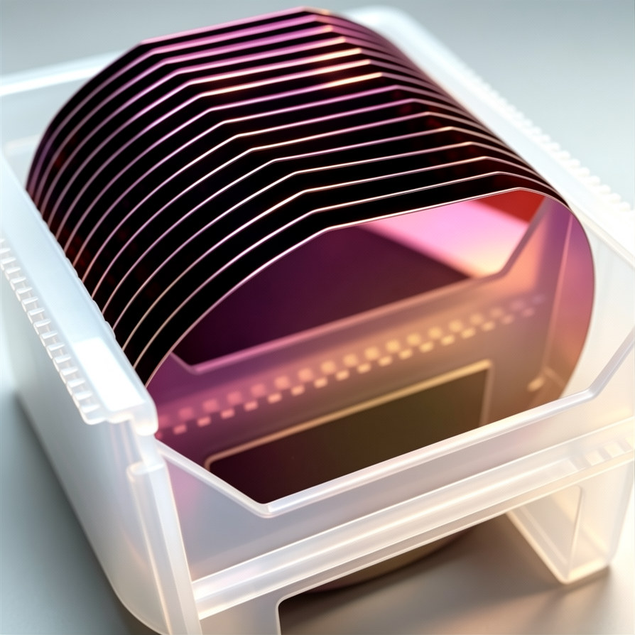
A silicon oxide wafer is a silicon substrate with a controlled SiO₂ layer thermally grown on its surface. It is widely used for insulation, passivation, masking and semiconductor device fabrication.
Dry oxidation produces a dense, high-quality oxide and is generally preferred for thin oxide layers. Wet oxidation has a higher growth rate and is typically used for thicker SiO₂ layers.
Yes. We support research, prototype and small-batch orders, as well as production requirements.
Please provide the wafer size, orientation, doping type, resistivity, SiO₂ thickness, oxidation method, oxidation side and quantity.
Technical Inquiry
Share your material, dimensions, specifications, application or project stage. Our team will review your requirements and respond within one business day.
Engineering-led response
Inquiries are routed to the appropriate technical or commercial team.
Address
No. 1389, Lianmei Road, Lianhua Industrial Zone, Tong’an, Xiamen, Fujian 361100, China
Phone


