01
Blue, Green & UV Laser Diodes (LDs)
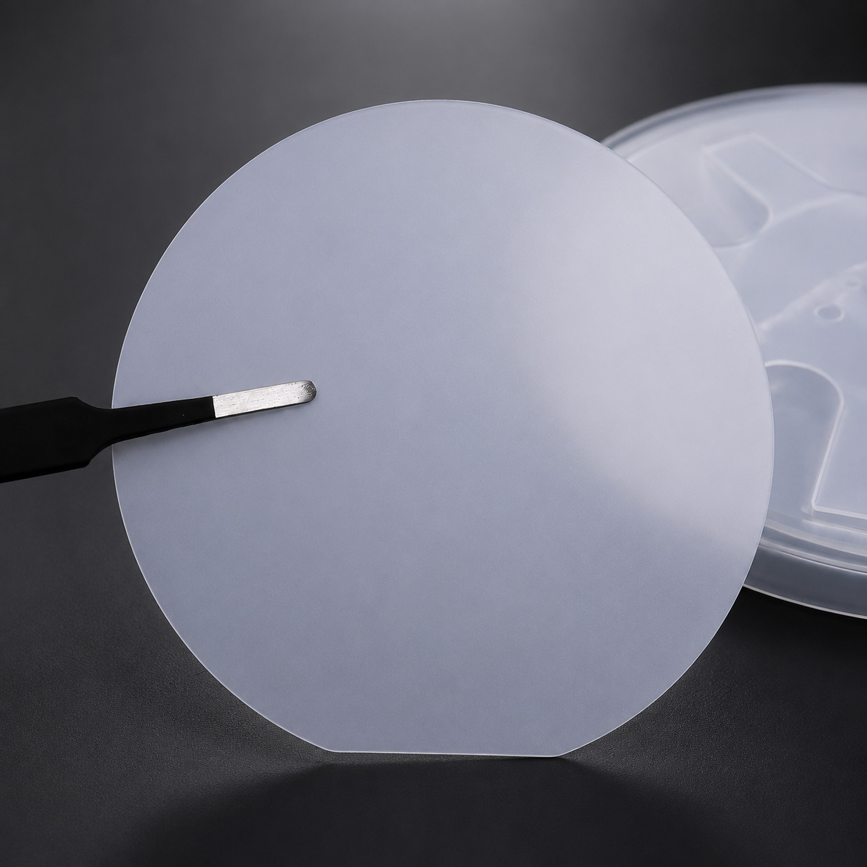
Low dislocation density (<5×10⁶ cm⁻²) enables high-efficiency, low-threshold current, and long-lifetime edge-emitting lasers and VCSELs for blue, green, and UV applications.

Select a wafer type to view detailed specs
Export of this product is regulated by the Ministry of Commerce of the PRC (MOFCOM). An export license must be obtained prior to shipment.
Export of this product is regulated by the Ministry of Commerce of the PRC (MOFCOM). An export license must be obtained prior to shipment.
Export of this product is regulated by the Ministry of Commerce of the PRC (MOFCOM). An export license must be obtained prior to shipment.
Low dislocation density (<5×10⁶ cm⁻²) enables high-efficiency, low-threshold current, and long-lifetime edge-emitting lasers and VCSELs for blue, green, and UV applications.
Native GaN platform providing uniform emission and high crystalline quality for next-generation AR/VR Micro-LED displays and ultra-high-brightness applications.
Excellent thermal conductivity and semi-insulating properties make it ideal for high-linearity, high-efficiency RF power amplifiers in 5G/6G infrastructure and millimeter-wave systems.
The definitive platform for exploring novel GaN device physics, quantum devices (quantum dots/wires), and next-generation optoelectronic concepts.
Quick answers on material selection, customization, testing and ordering.
The typical dislocation density is <5×10⁶ cm⁻². Specific values can be discussed according to the required wafer grade and application.
Yes. In addition to conventional c-plane GaN, we can provide a-plane, m-plane, semi-polar and non-polar substrates according to the requirements of the intended device structure.
Yes. PWG is R&D friendly. We provide both standard sizes (2-inch, 4-inch, 10x10mm²) and custom dimensions.
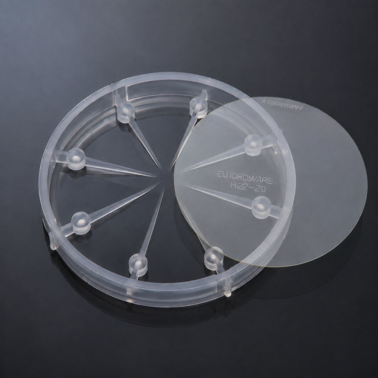
Wafers are vacuum-sealed in single-wafer cassettes within an cleanroom to ensure Fab-ready delivery.
Technical Inquiry
Share your material, dimensions, specifications, application or project stage. Our team will review your requirements and respond within one business day.
Engineering-led response
Inquiries are routed to the appropriate technical or commercial team.
Address
No. 1389, Lianmei Road, Lianhua Industrial Zone, Tong’an, Xiamen, Fujian 361100, China
Phone